Typical applications, Block diagram, At8xc51snd1c – Rainbow Electronics AT89C51SND1C User Manual
Page 2
2
AT8xC51SND1C
4109E–8051–06/03
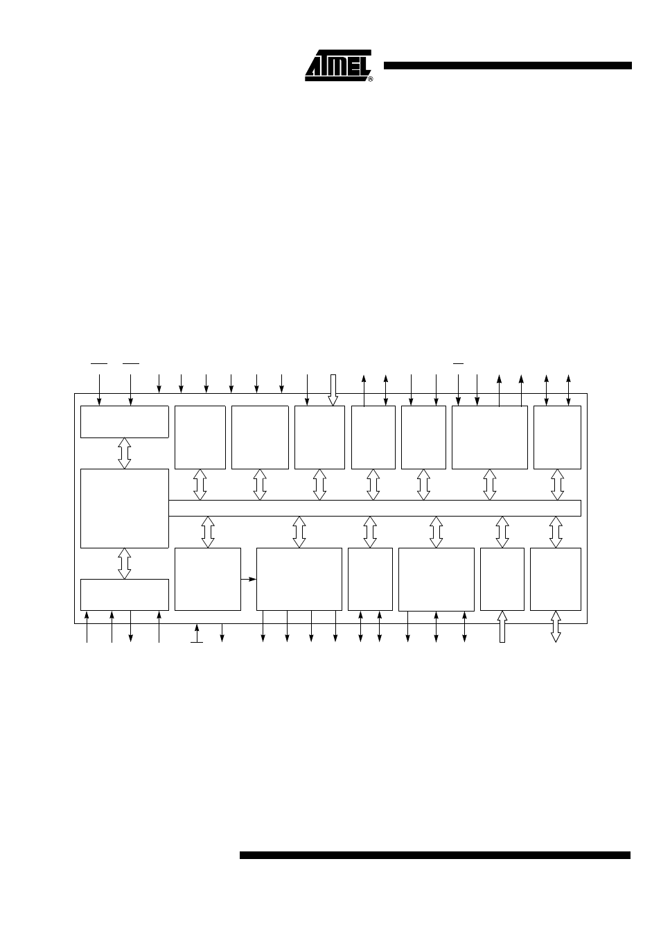
The AT83C51SND1C includes 64K Bytes of ROM memory.
The AT8xC51SND1C include 2304 Bytes of RAM memory.
The AT8xC51SND1C provides the necessary features for human interface like timers,
keyboard port, serial or parallel interface (USB, TWI, SPI, IDE), ADC input, I
2
S output,
and all external memory interface (NAND or NOR Flash, SmartMedia, MultiMedia,
DataFlash cards).
Typical Applications
•
MP3-Player
•
PDA, Camera, Mobile Phone MP3
•
Car Audio/Multimedia MP3
•
Home Audio/Multimedia MP3
Block Diagram
Figure 1. AT8xC51SND1C Block Diagram
8-Bit Internal Bus
Clock and PLL
Unit
C51 (X2 Core)
RAM
2304 Bytes
Flash
ROM
Interrupt
Handler Unit
FILT
X2
X1
MP3 Decoder
Unit
TWI
Controller
MMC
Interface
I/O
SCL SDA
MDAT
P0-P5
10-bit A to D
Converter
VSS
VDD
Keyboard
Interface
KIN3:0
I
2
S/PCM
Audio Interface
AVSS
AVDD
1
Alternate function of Port 1
AIN1:0
Ports
INT0
INT1
MOSI
MISO
3
Alternate function of Port 3
4
Alternate function of Port 4
Timers 0/1
T1
T0
SPI/DataFlash
Controller
MCLK
MCMD
SCK
RST
AREF
DSEL
DCLK
SCLK
DOUT
64 KBytes
USB
Controller
D+
D-
UART
RXD
TXD
IDE
Interface
SS
Watchdog
Flash Boot
4 KBytes
ISP
UVSS
UVDD
and
BRG
ALE
3
3
3
3
3
3
4
4
4
4
1
1
1
or
10-bit ADC