Figure 7, At8xc51snd1c – Rainbow Electronics AT89C51SND1C User Manual
Page 13
13
AT8xC51SND1C
4109E–8051–06/03
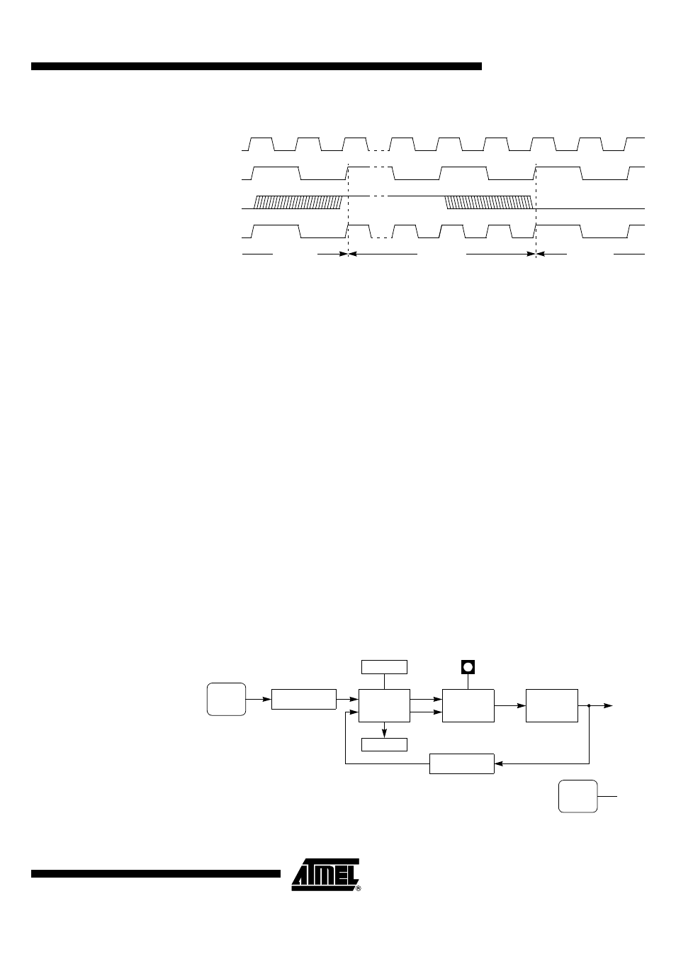
Figure 7. Mode Switching Waveforms
Note:
1. In order to prevent any incorrect operation while operating in X2 mode, user must be
aware that all peripherals using clock frequency as time reference (timers, etc.) will
have their time reference divided by 2. For example, a free running timer generating
an interrupt every 20 ms will then generate an interrupt every 10 ms.
PLL
PLL Description
The AT8xC51SND1C PLL is used to generate internal high frequency clock (the PLL
Clock) synchronized with an external low-frequency (the Oscillator Clock). The PLL
clock provides the MP3 decoder, the audio interface, and the USB interface clocks.
Figure 8 shows the internal structure of the PLL.
The PFLD block is the Phase Frequency Comparator and Lock Detector. This block
makes the comparison between the reference clock coming from the N divider and the
reverse clock coming from the R divider and generates some pulses on the Up or Down
signal depending on the edge position of the reverse clock. The PLLEN bit in PLLCON
register is used to enable the clock generation. When the PLL is locked, the bit PLOCK
in PLLCON register (see Table 17) is set.
The CHP block is the Charge Pump that generates the voltage reference for the VCO by
injecting or extracting charges from the external filter connected on PFILT pin (see
Fi g u re 9 ) . V a l u e o f t h e f i l t e r c o m p o n e n t s a r e d e t a i l e d i n th e S e c t i o n “ DC
Characteristics”.
The VCO block is the Voltage Controlled Oscillator controlled by the voltage V
ref
pro-
duced by the charge pump. It generates a square wave signal: the PLL clock.
Figure 8. PLL Block Diagram and Symbol
X1
÷
2
X1
Clock
X2 Bi
t
X2 Mode
(1)
STD Mode
STD Mode
PLLEN
PLLCON.1
N6:0
N divider
R divider
VCO
PLLclk
OSCclk
R
1
+
(
)
×
N
1
+
-----------------------------------------------
=
OSC
CLOCK
PFLD
PLOCK
PLLCON.0
PFILT
CHP
Vref
Up
Down
R9:0
PLL
CLOCK
PLL Clock Symbol
PLL
Clock