Flash memory architecture, At8xc51snd1c – Rainbow Electronics AT89C51SND1C User Manual
Page 18
18
AT8xC51SND1C
4109E–8051–06/03
User Space
This space is composed of a 64K Bytes ROM memory programmed during the manu-
facturing process. It contains the user’s application code.
Flash Memory
Architecture
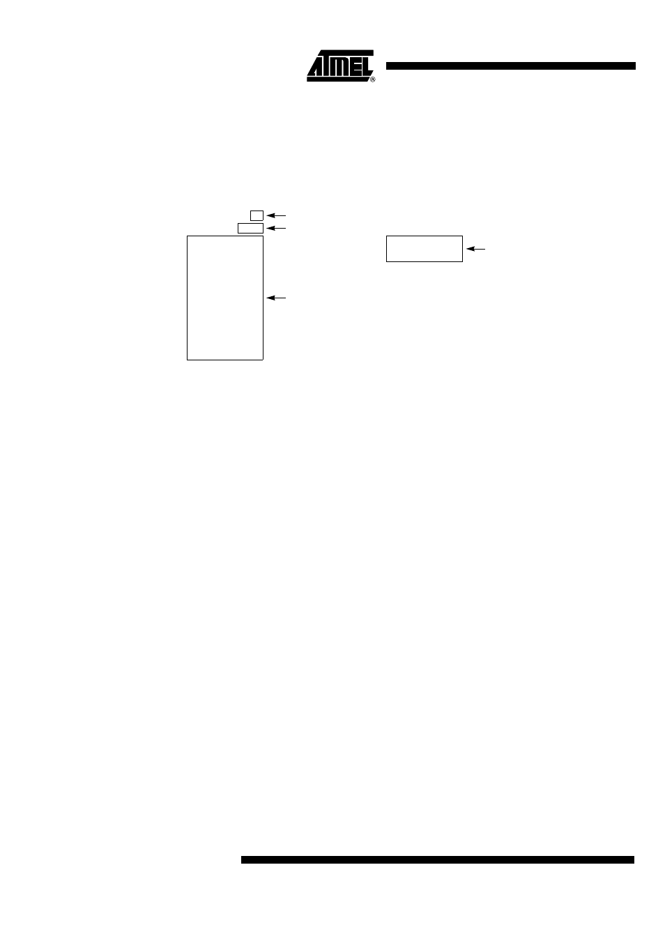
As shown in Figure 13 the AT89C51SND1C Flash memory is composed of four spaces
detailed in the following paragraphs.
Figure 13. AT89C51SND1C Memory Architecture
User Space
This space is composed of a 64K Bytes Flash memory organized in 512 pages of 128
Bytes. It contains the user’s application code.
This space can be read or written by both software and hardware modes.
Boot Space
This space is composed of a 4K Bytes Flash memory. It contains the boot loader for In-
System Programming and the routines for In Application Programming.
This space can only be read or written by hardware mode using a parallel programming
tool.
Hardware Security Space
This space is composed of one Byte: the Hardware Security Byte (HSB see Table 22)
divided in 2 separate nibbles. The MSN contains the X2 mode configuration bit and the
Boot Loader Jump Bit as detailed in Section “Boot Memory Execution”, page 19 and can
be written by software while the LSN contains the lock system level to protect the mem-
ory content against piracy as detailed in Section “Hardware Security System”, page 19
and can only be written by hardware.
Extra Row Space
This space is composed of 2 Bytes:
•
The Software Boot Vector (SBV, see Table 23).
This Byte is used by the software boot loader to build the boot address.
•
The Software Security Byte (SSB, see Table 24).
This Byte is used to lock the execution of some boot loader commands.
FFFFh
64K Bytes
Flash Memory
0000h
Hardware Security
User
4K Bytes
Flash Memory
FFFFh
F000h
Boot
Extra Row