Figure 154, Figure 154), At8xc51snd1c – Rainbow Electronics AT89C51SND1C User Manual
Page 198
198
AT8xC51SND1C
4109E–8051–06/03
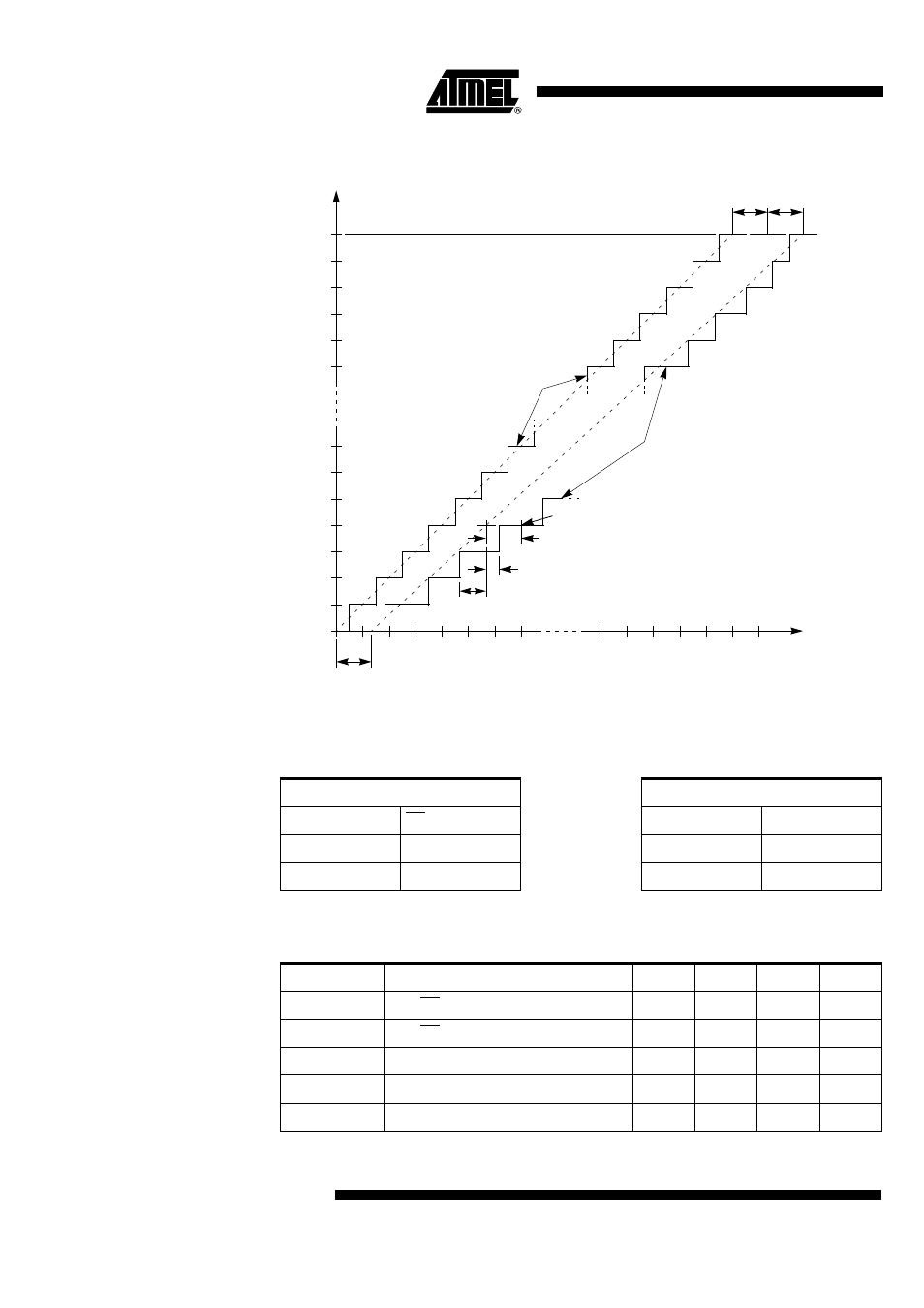
Figure 154. Analog to Digital Converter Characteristics
Flash Memory
Definition of symbols
Table 174. Flash Memory Timing Symbol Definitions
Timings
Table 175. Flash Memory AC Timing
V
DD
= 2.7 to 3.3 V, T
A
= -40 to +85
°
C
1
2
3
4
5
6
7
1018 1019 1020 1021 1022 1023 1024
1
2
3
4
5
6
7
1018
1019
1020
1021
1022
1023
Offset
Error OSe
Code Out
AVIN
Offset
Error
OSe
Gain
Error
Ge
Ideal Transfer curve
1 LSB
(ideal)
Integral non-linearity (ILe)
Differential non-linearity (DLe)
Center of a step
Example of an actual transfer curve
0
0
(LSB ideal)
Signals
Conditions
S
ISP
L
Low
R
RST
V
Valid
B
FBUSY flag
X
No Longer Valid
Symbol
Parameter
Min
Typ
Max
Unit
T
SVRL
Input ISP Valid to RST Edge
50
ns
T
RLSX
Input ISP Hold after RST Edge
50
ns
T
BHBL
FLASH Internal Busy (Programming) Time
10
ms
N
FCY
Number of Flash Write Cycles
100K
Cycle
T
FDR
Flash Data Retention Time
10
Years
- MAX5151 (16 pages)
- MAXQ3108 (64 pages)
- MAX5661 (39 pages)
- MAX6691 (7 pages)
- MAX5362 (12 pages)
- ADC10158 (26 pages)
- MAX8922L (14 pages)
- MAX8596Z (8 pages)
- MAX7491 (18 pages)
- MAX15040 (15 pages)
- MAX5177 (16 pages)
- ADC08138 (22 pages)
- MAX5961 (42 pages)
- T89C51RD2 (86 pages)
- MAX16055 (9 pages)
- MAX6659 (17 pages)
- ADC0820 (20 pages)
- MAX6678 (19 pages)
- MAX8884Z (15 pages)
- MAX16915 (9 pages)
- MAX8620 (18 pages)
- MAX5144 (12 pages)
- MAX6670 (8 pages)
- MAX8760 (39 pages)
- W78C32C (14 pages)
- MX7533 (8 pages)
- MAX8727 (13 pages)
- MAX9053 (15 pages)
- W78C54 (16 pages)
- MAX8614B (15 pages)
- W90N740 (219 pages)
- MAX6626 (13 pages)
- ADC10738 (30 pages)
- MAX17000 (31 pages)
- MAX5051 (21 pages)
- MAXQ1004 (18 pages)
- MAX6871 (51 pages)
- MX7847 (12 pages)
- MAX6608 (6 pages)
- MAX17083 (15 pages)
- MAX6641 (17 pages)
- MAX5251 (16 pages)
- MAX6338 (8 pages)
- MAX6690 (16 pages)
- MAX8668 (18 pages)