Internal pin structure, At8xc51snd1c – Rainbow Electronics AT89C51SND1C User Manual
Page 11
11
AT8xC51SND1C
4109E–8051–06/03
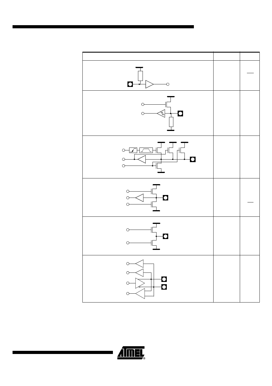
Internal Pin Structure
Table 15. Detailed Internal Pin Structure
Notes:
1. For information on resistors value, input/output levels, and drive capability, refer to
the Section “DC Characteristics”, page 181.
2. When the Two Wire controller is enabled, P
1
, P
2
, and P
3
transistors are disabled
allowing pseudo open-drain structure.
3. In Port 2, P
1
transistor is continuously driven when outputting a high level bit address
(A15:8).
Circuit
(1)
Type
Pins
Input
TST
Input/Output
RST
Input/Output
P1
(2)
P2
(3)
P3
P4
P53:0
Input/Output
P0
MCMD
MDAT
ISP
Output
ALE
SCLK
DCLK
DOUT
DSEL
MCLK
Input/Output
D+
D-
R
TS
T
VDD
R
RS
T
VSS
P
VDD
Watchdog Output
P
3
VSS
N
P
1
VDD
VDD
2 osc
Latch Output
periods
P
2
VDD
VSS
N
P
VDD
VSS
N
P
VDD
D+
D-
See also other documents in the category Rainbow Electronics Sensors:
- MAX5151 (16 pages)
- MAXQ3108 (64 pages)
- MAX5661 (39 pages)
- MAX6691 (7 pages)
- MAX5362 (12 pages)
- ADC10158 (26 pages)
- MAX8922L (14 pages)
- MAX8596Z (8 pages)
- MAX7491 (18 pages)
- MAX15040 (15 pages)
- MAX5177 (16 pages)
- ADC08138 (22 pages)
- MAX5961 (42 pages)
- T89C51RD2 (86 pages)
- MAX16055 (9 pages)
- MAX6659 (17 pages)
- ADC0820 (20 pages)
- MAX6678 (19 pages)
- MAX8884Z (15 pages)
- MAX16915 (9 pages)
- MAX8620 (18 pages)
- MAX5144 (12 pages)
- MAX6670 (8 pages)
- MAX8760 (39 pages)
- W78C32C (14 pages)
- MX7533 (8 pages)
- MAX8727 (13 pages)
- MAX9053 (15 pages)
- W78C54 (16 pages)
- MAX8614B (15 pages)
- W90N740 (219 pages)
- MAX6626 (13 pages)
- ADC10738 (30 pages)
- MAX17000 (31 pages)
- MAX5051 (21 pages)
- MAXQ1004 (18 pages)
- MAX6871 (51 pages)
- MX7847 (12 pages)
- MAX6608 (6 pages)
- MAX17083 (15 pages)
- MAX6641 (17 pages)
- MAX5251 (16 pages)
- MAX6338 (8 pages)
- MAX6690 (16 pages)
- MAX8668 (18 pages)