At8xc51snd1c – Rainbow Electronics AT89C51SND1C User Manual
Page 10
10
AT8xC51SND1C
4109E–8051–06/03
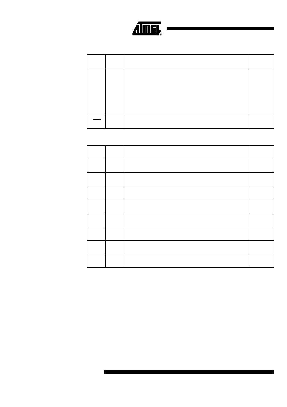
Table 13. System Signal Description
Table 14. Power Signal Description
Signal
Name
Type
Description
Alternate
Function
RST
I
Reset Input
Holding this pin high for 64 oscillator periods while the oscillator is
running resets the device. The Port pins are driven to their reset
conditions when a voltage lower than V
IL
is applied, whether or not the
oscillator is running.
This pin has an internal pull-down resistor which allows the device to be
reset by connecting a capacitor between this pin and V
DD
.
Asserting RST when the chip is in Idle mode or Power-Down mode
returns the chip to normal operation.
-
TST
I
Test Input
Test mode entry signal. This pin must be set to V
DD
.
-
Signal
Name
Type
Description
Alternate
Function
VDD
PWR
Digital Supply Voltage
Connect these pins to +3V supply voltage.
-
VSS
GND
Circuit Ground
Connect these pins to ground.
-
AVDD
PWR
Analog Supply Voltage
Connect this pin to +3V supply voltage.
-
AVSS
GND
Analog Ground
Connect this pin to ground.
-
PVDD
PWR
PLL Supply voltage
Connect this pin to +3V supply voltage.
-
PVSS
GND
PLL Circuit Ground
Connect this pin to ground.
-
UVDD
PWR
USB Supply Voltage
Connect this pin to +3V supply voltage.
-
UVSS
GND
USB Ground
Connect this pin to ground.
-