Analog to digital converter, Description, At8xc51snd1c – Rainbow Electronics AT89C51SND1C User Manual
Page 174
174
AT8xC51SND1C
4109E–8051–06/03
Analog to Digital
Converter
The AT8xC51SND1C implement a 2-channel 10-bit (8 true bits) analog to digital con-
verter (ADC). First channel of this ADC can be used for battery monitoring while the
second one can be used for voice sampling at 8 kHz.
Description
The A/D converter interfaces with the C51 core through four special function registers:
ADCON, the ADC control register (see Table 147); ADDH and ADDL, the ADC data reg-
isters (see Table 149 and Table 150); and ADCLK, the ADC clock register (see
Table 148).
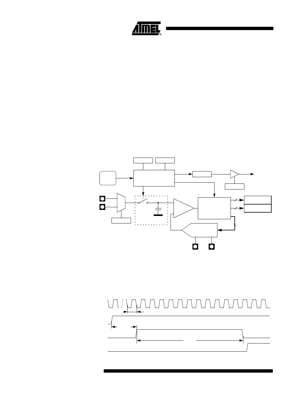
As shown in Figure 129, the ADC is composed of a 10-bit cascaded potentiometric digi-
tal to analog converter, connected to the negative input of a comparator. The output
voltage of this DAC is compared to the analog voltage stored in the Sample and Hold
and coming from AIN0 or AIN1 input depending on the channel selected (see
Table 146). The 10-bit ADDAT converted value (see formula in Figure 129) is delivered
in ADDH and ADDL registers, ADDH is giving the 8 most significant bits while ADDL is
giving the 2 least significant bits. ADDAT
Figure 129. ADC Structure
Figure 130 shows the timing diagram of a complete conversion. For simplicity, the figure
depicts the waveforms in idealized form and do not provide precise timing information.
For ADC characteristics and timing parameters refer to the section “AC Characteristics”.
Figure 130. Timing Diagram
0
1
AIN1
AIN0
ADCS
ADCON.0
AVSS
Sample and Hold
ADDH
AREFP
R/2R DAC
ADC
CLOCK
AREFN
8
10
ADEN
ADCON.5
ADSST
ADCON.3
ADEOC
ADCON.4
ADC
Interrupt
Request
EADC
IEN1.3
CONTROL
+
-
ADDL
2
SAR
ADDAT
1023 V
⋅
IN
V
REF
---------------------------
=
ADEN
ADSST
ADEOC
T
SETUP
T
CONV
CLK
T
ADCLK