Synchronous peripheral interface, At8xc51snd1c – Rainbow Electronics AT89C51SND1C User Manual
Page 146
146
AT8xC51SND1C
4109E–8051–06/03
Synchronous
Peripheral Interface
The AT8xC51SND1C implements a Synchronous Peripheral Interface with master and
slave modes capability.
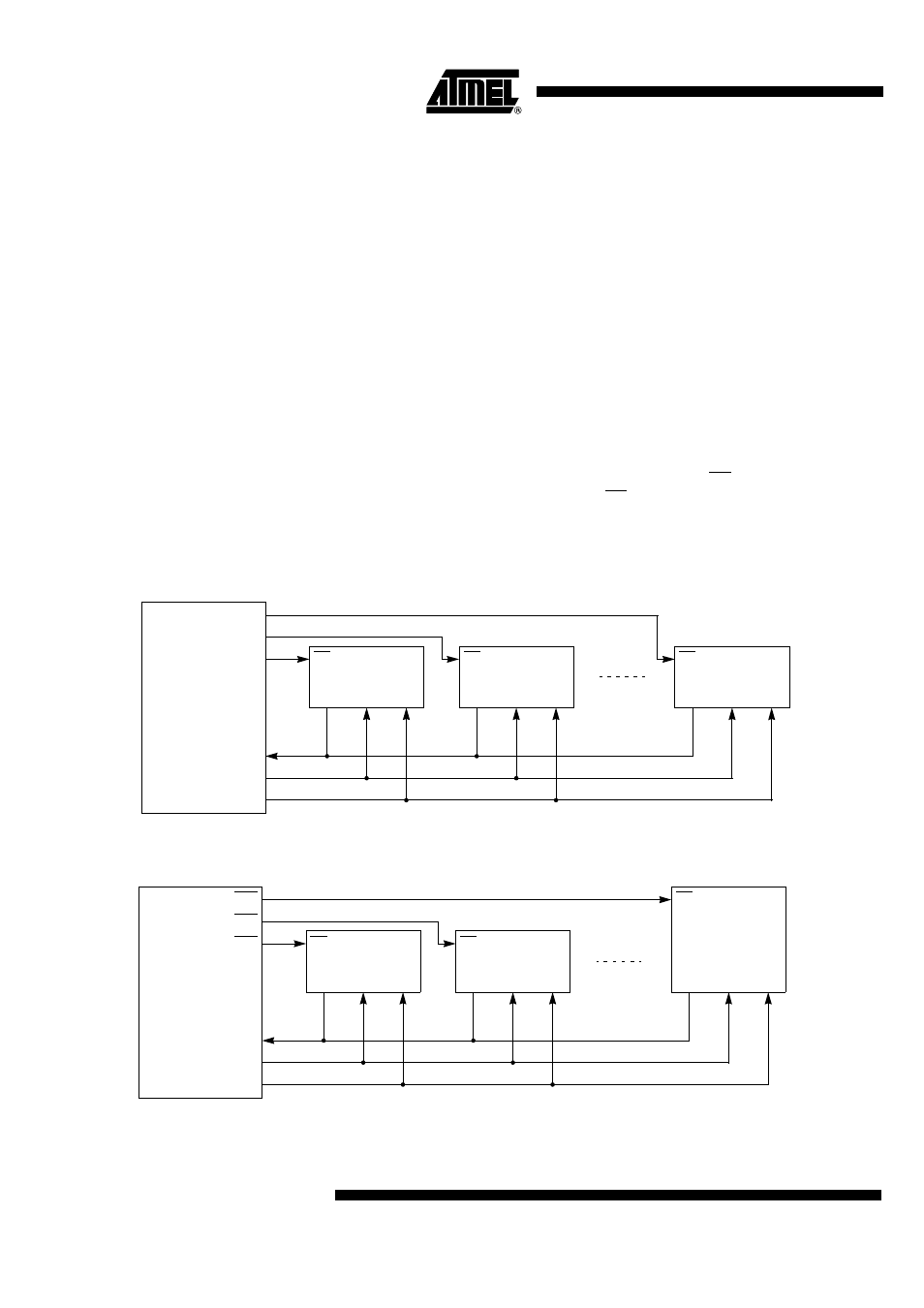
Figure 111 shows an SPI bus configuration using the AT8xC51SND1C as master con-
nected to slave peripherals while Figure 112 shows an SPI bus configuration using the
AT8xC51SND1C as slave of an other master.
The bus is made of three wires connecting all the devices together:
•
Master Output Slave Input (MOSI): it is used to transfer data in series from the
master to a slave.
It is driven by the master.
•
Master Input Slave Output (MISO): it is used to transfer data in series from a slave
to the master.
It is driven by the selected slave.
•
Serial Clock (SCK): it is used to synchronize the data transmission both in and out
the devices through their MOSI and MISO lines. It is driven by the master for eight
clock cycles which allows to exchange one Byte on the serial lines.
Each slave peripheral is selected by one Slave Select pin (SS). If there is only one
slave, it may be continuously selected with SS tied to a low level. Otherwise, the
AT8xC51SND1C may select each device by software through port pins (Pn.x). Special
care should be taken not to select 2 slaves at the same time to avoid bus conflicts.
Figure 111. Typical Master SPI Bus Configuration
Figure 112. Typical Slave SPI Bus Configuration
AT8xC51SND1C
DataFlash 1
SS
MISO
MOSI
SCK
P4.0
P4.1
P4.2
Pn.z
Pn.y
Pn.x
SO
SI
SCK
DataFlash 2
SS
SO
SI
SCK
LCD
Controller
SS
SO
SI
SCK
MASTER
Slave 1
SS
MISO
MOSI
SCK
SSn
SS1
SS0
SO
SI
SCK
Slave 2
SS
SO
SI
SCK
AT8xC51SND1C
Slave n
SS
MISO MOSI SCK