Texas Instruments TMS320C64x DSP User Manual
Page 214
Video Display Registers
4-69
Video Display Port
SPRU629
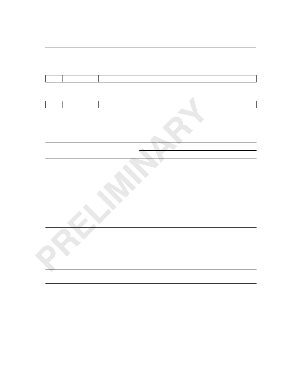
Figure 4–47. Video Display Field 1 Image Offset Register (VDIMGOFF1)
31
30
28
27
16
NV
Reserved
IMGVOFF1
R/W-0
R-0
R/W-0
15
14
12
11
0
NH
Reserved
IMGHOFF1
R/W-0
R-0
R/W-0
Legend: R = Read only; R/W = Read/Write; -n = value after reset
Table 4–14. Video Display Field 1 Image Offset Register (VDIMGOFF1) Field Descriptions
Description
Bit
field
†
symval
†
Value
BT.656 and Y/C Mode
Raw Data Mode
31
NV
Negative vertical image offset enable bit.
NONE
0
Not used.
NEGOFF
1
Display image window
begins before the first active
line of field 1. (Used for VBI
data output.)
Not used.
30–28
Reserved
–
0
Reserved. The reserved bit location is always read as 0. A
value written to this field has no effect.
27–16
IMGVOFF1
OF(value)
0–FFFh
Specifies the display image vertical offset in lines from the
first active line of field 1.
15
NH
Negative horizontal image offset.
NONE
0
Not used.
NEGOFF
1
Display image window
begins before the start of
active video. (Used for
HANC data output.)
Not used.
14–12
Reserved
–
0
Reserved. The reserved bit location is always read as 0. A
value written to this field has no effect.
11–0
IMGHOFF1
OF(value)
0–FFFh
Specifies the display image
horizontal offset in pixels
from the start of each line of
active video in field 1. This
must be an even number
(the LSB is treated as 0).
Specifies the display image
horizontal offset in pixels
from the start of each line of
active video in field 1.
† For CSL implementation, use the notation VP_VDIMGOFF1_field_symval