4 functional description, 1 general, 4 functional description -16 – Freescale Semiconductor ColdFire MCF52210 User Manual
Page 306: 1 general -16, 9 cfmclksel — cfm clock select register
ColdFire Flash Module (CFM)
MCF52211 ColdFire® Integrated Microcontroller Reference Manual, Rev. 2
18-16
Freescale Semiconductor
18.3.3.9
CFMCLKSEL — CFM Clock Select Register
The CFMCLKSEL register reflects the factory setting for read access latency from the system bus to the
flash block.
Figure 18-13. CFM Clock Select Register (CFMCLKSEL)
CFMCLKSEL register bits [1:0] are read-only, while the remaining bits read 0 and are not writable.
18.4
Functional Description
18.4.1
General
The following modes and operations are described in the corresponding sections:
1. Flash normal mode (
Section 18.4.2, “Flash Normal Mode”
)
a) Read operation (
Section 18.4.2.1, “Read Operation”
)
b) Write operation (
Section 18.4.2.2, “Write Operation”
)
c) Program, erase, and verify operations (
Section 18.4.2.3, “Program, Erase, and Verify
)
d) Stop mode (
)
2. Flash security operation (
Section 18.4.3, “Flash Security Operation”
)
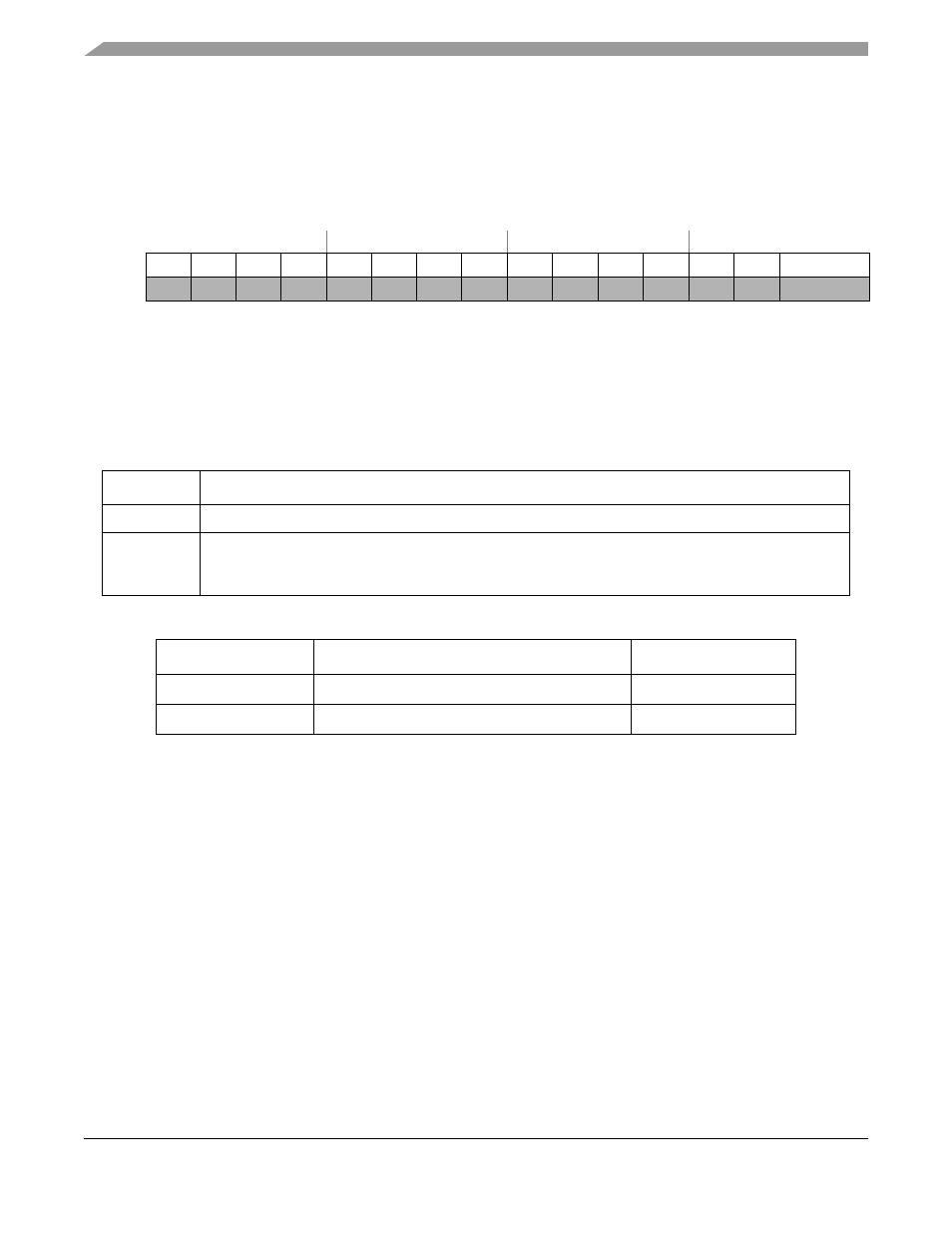
IPSBAR
Offset: 0x1D_004A(CFMCLKSEL)
Access: User read/write
15
14
13
12
11
10
9
8
7
6
5
4
3
2
1
0
R
0
0
0
0
0
0
0
0
0
0
0
0
0
0
CLKSEL
W
Reset
0
0
0
0
0
0
0
0
0
0
0
0
0
0
F
1
1
Reset state set by factory.
F
1
Table 18-14. CFMCLKSEL Field Descriptions
Field
Description
15 - 2
Reserved, should read 0
1 - 0
CLKSEL
Flash Read Access Latency Select
The CLKSEL bits set the read access latency to the flash block.
describes the setting that
selects between single-cycle and two-cycle flash block read access.
Table 18-15. Clock Select States
CLKSEL[1:0]
Description
Burst Read Access
2’b10
Single-Cycle Flash Block Read Access
1-1-1-1
All other combinations
Two-cycle Flash Block Read Access
2-1-1-1