Freescale Semiconductor ColdFire MCF52210 User Manual
Page 181
System Control Module (SCM)
MCF52211 ColdFire® Integrated Microcontroller Reference Manual, Rev. 2
Freescale Semiconductor
12-5
known as a ping-pong scheme) may load data into one portion of the dual-ported SRAM while the
processor is manipulating data in another portion of the SRAM. After the processor completes the data
calculations, it begins processing the recently-loaded buffer while the DMA moves out the
recently-calculated data from the other buffer, and reloads the next data block into the recently-freed
memory region. The process repeats with the processor and the DMA ping-ponging between alternate
regions of the dual-ported SRAM.
The device design implements the dual-ported SRAM in the memory space defined by the RAMBAR
register. There are two physical copies of the RAMBAR register: one located in the processor core and
accessible only via the privileged MOVEC instruction at CPU space address 0xC05 and another located
in the SCM at IPSBAR + 0x008. ColdFire core accesses to this memory are controlled by the
processor-local copy of the RAMBAR, while module accesses are enabled by the SCM's RAMBAR.
The physical base address programmed in both copies of the RAMBAR is typically the same value;
however, they can be programmed to different values. By definition, the base address must be a
0-modulo-size value.
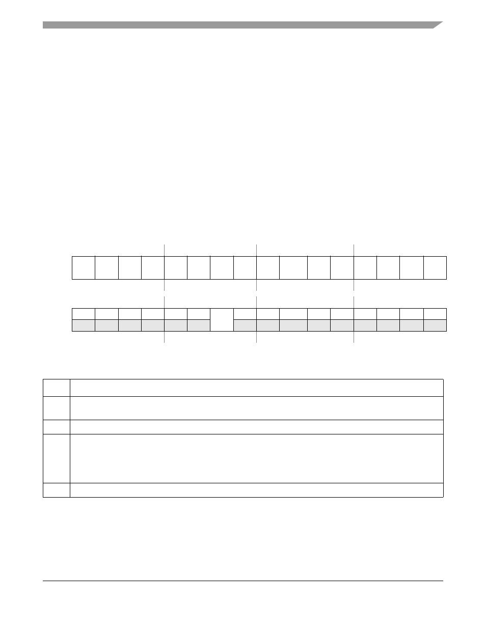
The SRAM modules are configured through the RAMBAR shown in
.
•
RAMBAR specifies the base address of the SRAM.
•
All undefined bits are reserved. These bits are ignored during writes to the RAMBAR and return
zeros when read.
IPSBAR
Offset: 0x0008 (RAMBAR)
Access: read/write
31
30
29
28
27
26
25
24
23
22
21
20
19
18
17
16
R
BA31 BA30 BA29 BA28 BA27 BA26 BA25 BA24 BA23
BA22
BA21 BA20 BA19 BA18 BA17 BA16
W
Reset
0
0
0
0
0
0
0
0
0
0
0
0
0
0
0
0
15
14
13
12
11
10
9
8
7
6
5
4
3
2
1
0
R
0
0
0
0
0
0
BDE
0
0
0
0
0
0
0
0
0
W
Reset
0
0
0
0
0
0
0
0
0
0
0
0
0
0
0
0
Figure 12-2. Memory Base Address Register (RAMBAR)
Table 12-4. RAMBAR Field Description
Field
Description
31–16
BA
Base address. Defines the memory module's base address on a 64-Kbyte boundary corresponding to the physical
array location within the 4 Gbyte address space supported by ColdFire.
15–10 Reserved, should be cleared.
9
BDE
Back door enable. Qualifies the module accesses to the memory.
0 Disables module accesses to the module.
1 Enables module accesses to the module.
NOTE: The SPV bit in the CPU’s RAMBAR must also be set to allow dual port access to the SRAM. For more
information, see
Section 5.2.1, “SRAM Base Address Register (RAMBAR)
.”
8–0
Reserved, should be cleared.