2 source address registers (sarn), 3 destination address registers (darn), 2 source address registers (sar n – Freescale Semiconductor ColdFire MCF52210 User Manual
Page 279: 3 destination address registers (dar, 2 source address registers (sar n ), 3 destination address registers (dar n )
DMA Controller Module
MCF52211 ColdFire® Integrated Microcontroller Reference Manual, Rev. 2
Freescale Semiconductor
17-5
17.3.2
Source Address Registers (SARn)
SARn, shown in
, contains the address from which the DMA controller requests data.
NOTE
The backdoor enable bit must be set in the SCM RAMBAR as well as the
secondary port valid bit in the core RAMBAR to enable backdoor accesses
from the DMA to SRAM. See
Section 5.2.1, “SRAM Base Address Register
for more details.
17.3.3
Destination Address Registers (DARn)
DARn, shown in
, holds the address to which the DMA controller sends data.
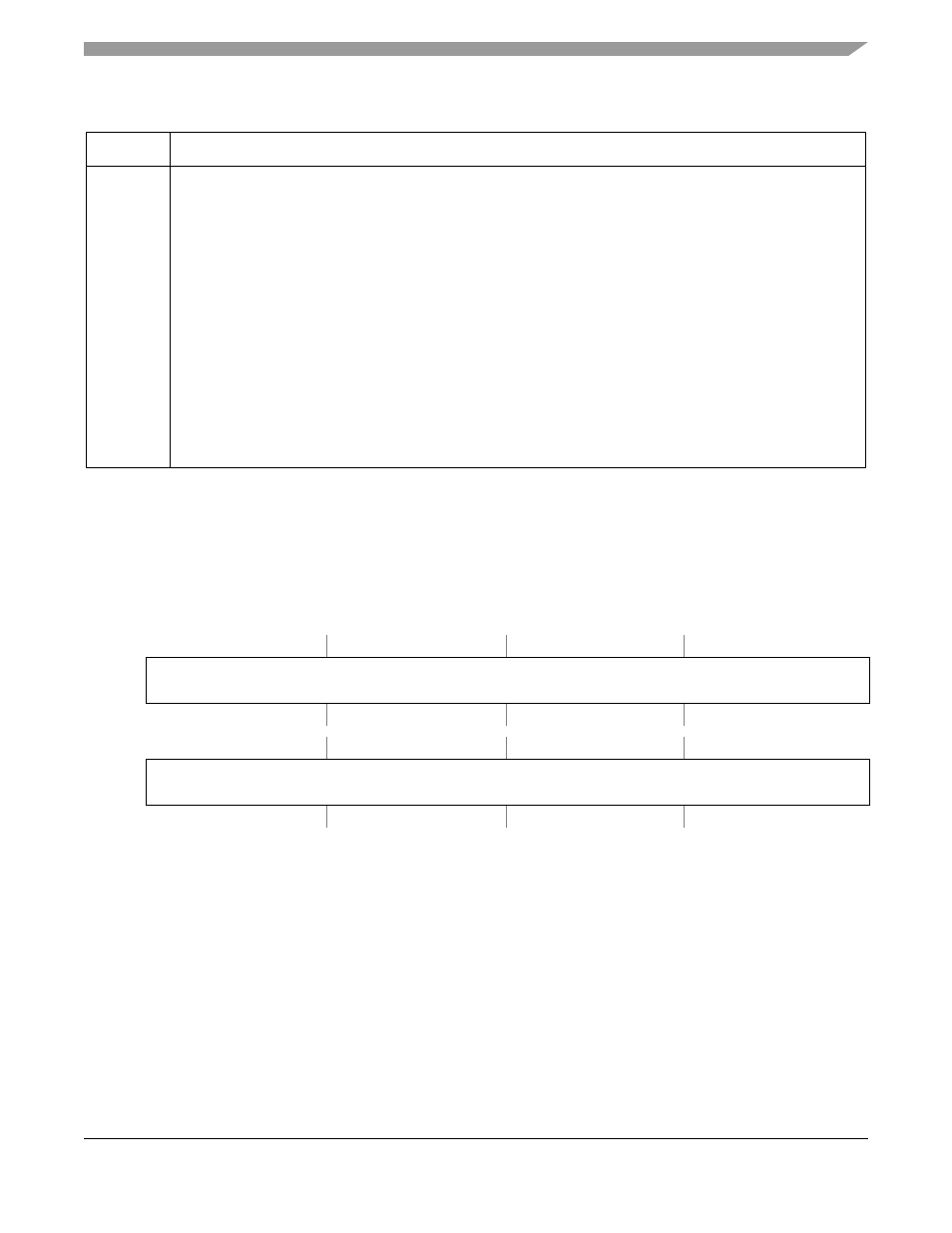
Table 17-2. DMAREQC Field Description
Field
Description
15–0
DMACn
DMA channel n. Each four bit field defines the logical connection between the DMA requesters and that DMA
channel.There are ten possible requesters (4 DMA Timers and 6 UARTs). Any request can be routed to any of
the DMA channels. Effectively, the DMAREQC provides a software-controlled routing matrix of the 10 DMA
request signals to the 4 channels of the DMA module. DMAC3 controls DMA channel 3, DMAC2 controls DMA
channel 2, etc.
0100 DMA Timer 0.
0101 DMA Timer 1.
0110 DMA Timer 2.
0111 DMA Timer 3.
1000 UART0 Receive.
1001 UART1 Receive.
1010 UART2 Receive.
1100 UART0 Transmit.
1101 UART1 Transmit.
1110 UART2 Transmit.
All other values are reserved and do not generate a DMA request.
IPSBAR
Offsets:
0x00_0100 (SAR0)
0x00_0110 (SAR1)
0x00_0120 (SAR2)
0x00_0130 (SAR3)
Access: read/write
31
30
29
28
27
26
25
24
23
22
21
20
19
18
17
16
R
SAR
W
Reset
0
0
0
0
0
0
0
0
0
0
0
0
0
0
0
0
15
14
13
12
11
10
9
8
7
6
5
4
3
2
1
0
R
SAR
W
Reset
0
0
0
0
0
0
0
0
0
0
0
0
0
0
0
0
Figure 17-4. Source Address Registers (SARn)