2 memory map/register definition, 2 memory map/register definition -2 – Freescale Semiconductor ColdFire MCF52210 User Manual
Page 476
Pulse-Width Modulation (PWM) Module
MCF52211 ColdFire® Integrated Microcontroller Reference Manual, Rev. 2
27-2
Freescale Semiconductor
Main features include the following:
•
Double-buffered period and duty cycle
•
Left- or center-aligned outputs
•
Eight independent PWM modules
•
Byte-wide registers provide programmable duty cycle and period control
•
Four programmable clock sources
NOTE
The GPIO module must be configured to enable the peripheral function of
the appropriate pins (refer to
Chapter 13, “General Purpose I/O Module”
)
prior to configuring the PWM module.
27.2
Memory Map/Register Definition
This section describes the registers and control bits in the PWM module. There are eight independent
PWM modules, each with its own control and counter registers. The memory map for the PWM is shown
below.
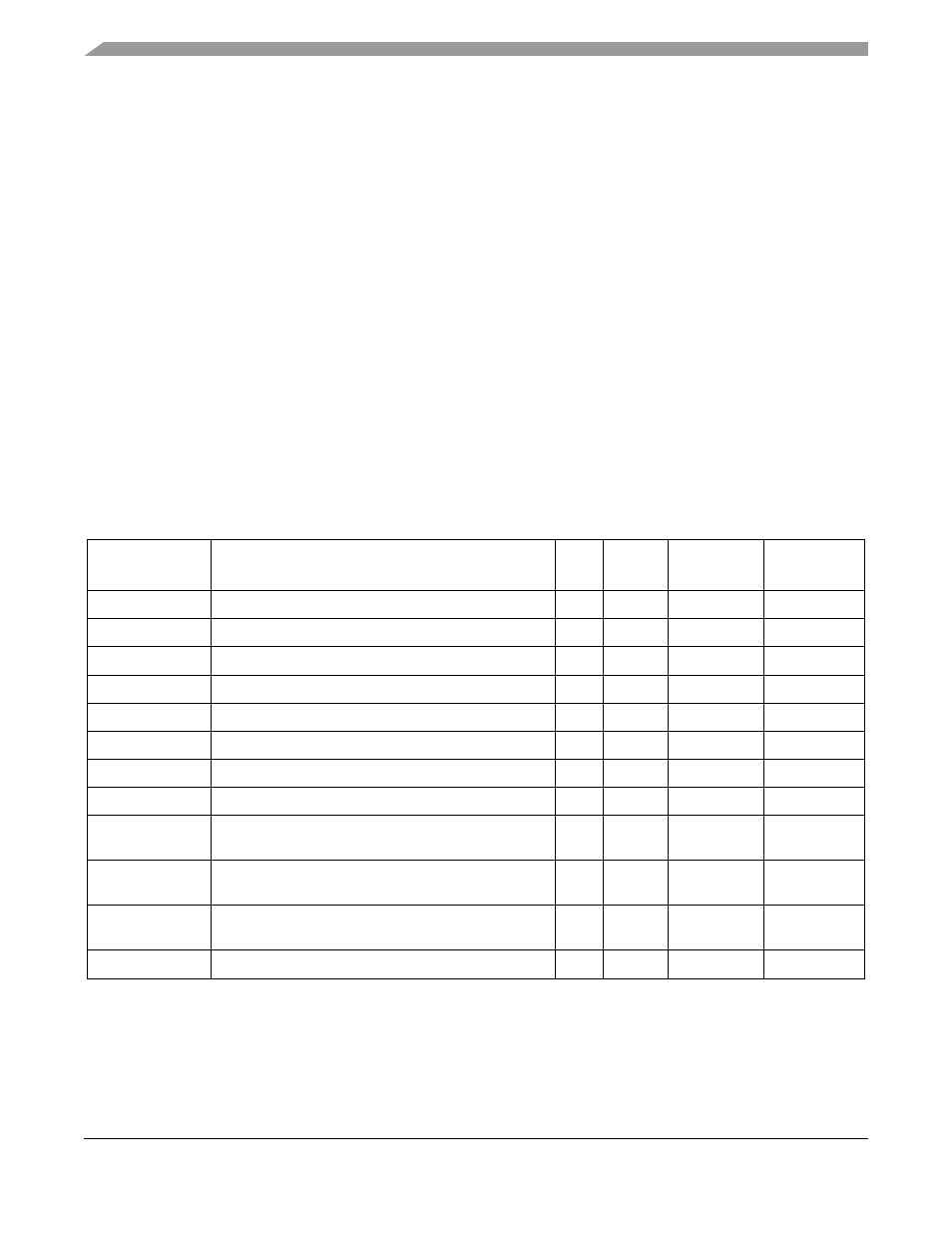
Table 27-1. PWM Memory Map
IPSBAR Offset
1,2
1
Addresses not assigned to a register and undefined register bits are reserved for expansion. Write accesses to these
reserved address spaces and reserved register bits have no effect.
2
A 32-bit access to any of these registers results in a bus transfer error.
Register
Width
(bits)
Access
Reset Value
Section/Page
0x1B_0000
PWM Enable Register (PWME)
8
R/W
0x00
0x1B_0001
PWM Polarity Register (PWMPOL)
8
R/W
0x00
0x1B_0002
PWM Clock Select Register (PWMCLK)
8
R/W
0x00
0x1B_0003
PWM Prescale Clock Select Register (PWMPRCLK)
8
R/W
0x00
0x1B_0004
PWM Center Align Enable Register (PWMCAE)
8
R/W
0x00
0x1B_0005
PWM Control Register (PWMCTL)
8
R/W
0x00
0x1B_0008
PWM Scale A Register (PWMSCLA)
8
R/W
0x00
0x1B_0009
PWM Scale B Register (PWMSCLB)
8
R/W
0x00
0x1B_000C + n
n = 0–7
PWM Channel n Counter Register (PWMCNTn)
8
R/W
0x00
0x1B_0014 + n
n = 0–7
PWM Channel n Period Register (PWMPERn)
8
R/W
0xFF
0x1B_001C + n
n = 0–7
PWM Channel n Duty Register (PWMDTYn)
8
R/W
0xFF
0x1B_0024
PWM Shutdown Register (PWMSDN)
8
R/W
0x00