5 pin assignment registers, 5 pin assignment registers -10, Figure 13-19 – Freescale Semiconductor ColdFire MCF52210 User Manual
Page 204: Figure 13-20, Figure 13-21, Table 13-5
General Purpose I/O Module
MCF52211 ColdFire® Integrated Microcontroller Reference Manual, Rev. 2
13-10
Freescale Semiconductor
13.6.5
Pin Assignment Registers
All pin assignment registers are read/write. Refer to
for the different functions assignable to each
pin.
Some signals can be assigned to different pins (see
). However, a signal should not be assigned
to more than one pin at the same time. If a signal is assigned to two or more pins simultaneously, the result
is undefined.
IPSBAR
Offset: 0x10_0054 (CLRQS)
Access: User read/write
7
6
5
4
3
2
1
0
R
0
CLRn6
CLRn5
CLRn4
CLRn3
CLRn2
CLRn1
CLRn0
W
Reset:
0
0
0
0
0
0
0
0
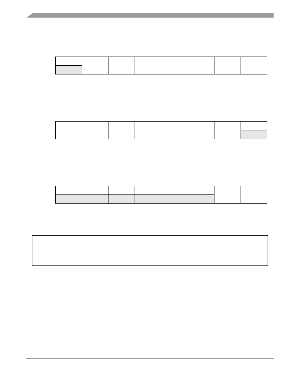
Figure 13-19. Port QS Clear Output Data Register (CLRQS)
IPSBAR
Offset: 0x10_0050 (CLRNQ)
Access: User read/write
7
6
5
4
3
2
1
0
R
CLRn7
CLRn6
CLRn5
CLRn4
CLRn3
CLRn2
CLRn1
0
W
Reset:
0
0
0
0
0
0
0
0
Figure 13-20. Port NQ Clear Output Data Register (CLRNQ)
IPSBAR
Offset: 0x10_0053 (CLRAS)
Access: User read/write
7
6
5
4
3
2
1
0
R
0
0
0
0
0
0
CLRn1
CLRn0
W
Reset:
0
0
0
0
0
0
0
0
Figure 13-21. Port AS Clear Output Data Register (CLRAS)
Table 13-5. CLRn Field Descriptions
Field
Description
CLRnx
Portnx pin data/set data bits.
1 Never returned for reads; no effect for writes
0 Always returned for reads; clears corresponding port nx bit for writes