2 signal overview, Signal overview, Table 9: signal overview – BECKHOFF ET1100 User Manual
Page 26
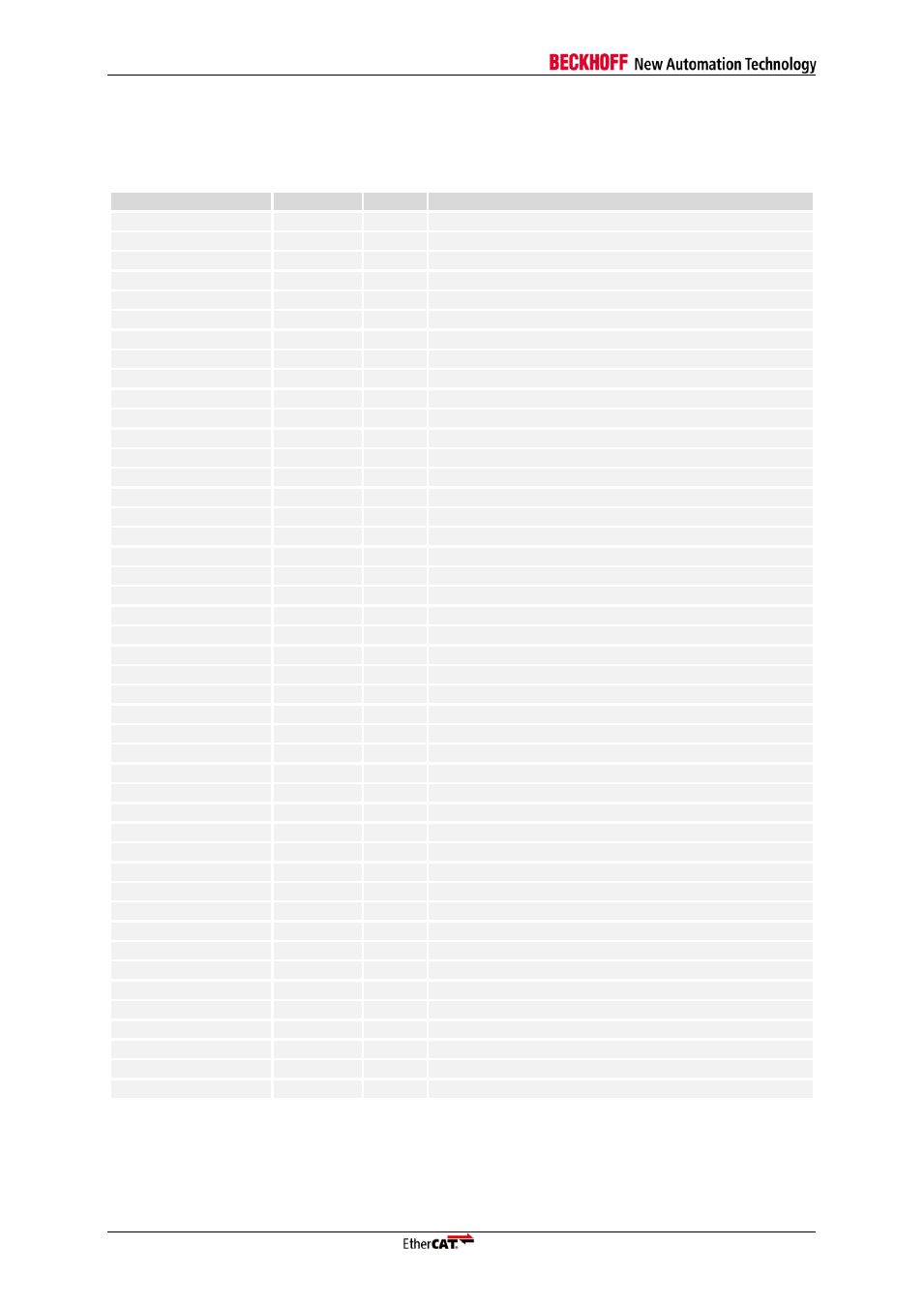
Pin Description
III-12
Slave Controller
– ET1100 Hardware Description
3.1.2
Signal Overview
Table 9: Signal Overview
Signal
Type
Dir.
Description
C25_ENA
Configuration
I
CLK25OUT2 Enable: Enable CLK25OUT2
C25_SHI[1:0]
Configuration
I
TX Shift: Shifting/phase compensation of MII TX signals
CLK_MODE[1:0]
Configuration
I
CPU_CLK configuration
CLK25OUT1/CLK25OUT2
MII
O
25 MHz clock source for Ethernet PHYs
CPU_CLK
PDI
O
Clock signal for µController
CTRL_STATUS_MOVE
Configuration
I
Move Digital I/O Control/Status signal to last available PDI byte
EBUS(3:0)-RX-
EBUS
LI-
EBUS LVDS receive signal -
EBUS(3:0)-RX+
EBUS
LI+
EBUS LVDS receive signal +
EBUS(3:0)-TX-
EBUS
LO-
EBUS LVDS transmit signal -
EBUS(3:0)-TX+
EBUS
LO+
EBUS LVDS transmit signal +
EEPROM_CLK
EEPROM
BD
EEPROM I
2
C Clock
EEPROM_DATA
EEPROM
BD
EEPROM I
2
C Data
EEPROM_SIZE
Configuration
I
EEPROM size configuration
PERR(3:0)
LED
O
Port receive error LED output (for testing)
GND
Core
Power
Core logic ground
GND
I/O
Power
I/O ground
GND
PLL
Power
PLL ground
LINK_MII(3:0)
MII
I
PHY signal indicating a link
LINKACT(3:0)
LED
O
Link/Activity LED output
LINKPOL
Configuration
I
LINK_MII(3:0) polarity configuration
MI_CLK
MII
O
PHY Management Interface clock
MI_DATA
MII
BD
PHY Management Interface data
OSC_IN
Clock
I
Clock source (crystal/oscillator)
OSC_OUT
Clock
O
Clock source (crystal)
P_CONF(3:0)
Configuration
I
Physical layer of logical ports
P_MODE[1:0]
Configuration
I
Number of physical ports and corresponding logical ports
PDI[39:0]
PDI
BD
PDI signal, depending on EEPROM content
PHYAD_OFF
Configuration
I
Ethernet PHY Address Offset
RBIAS
EBUS
BIAS resistor for LVDS TX current adjustment
Res. [7:0]
Reserved
I
Reserved pins
RESET
General
BD
Open collector Reset output/Reset input
RUN
LED
O
Run LED controlled by AL Status register
RX_CLK(3:0)
MII
I
MII receive clock
RX_D(3:0)[3:0]
MII
I
MII receive data
RX_DV(3:0)
MII
I
MII receive data valid
RX_ERR(3:0)
MII
I
MII receive error
SYNC/LATCH[1:0]
DC
I/O
Distributed Clocks SyncSignal output or LatchSignal input
TESTMODE
General
I
Reserved for testing, connect to GND
TRANS(3:0)
MII
I
MII interface sharing: share port enable
TRANS_MODE_ENA
Configuration
I
Enable MII interface sharing (and TRANS(3:0) signals)
TX_D(3:0)[3:0]
MII
O
MII transmit data
TX_ENA(3:0)
MII
O
MII transmit enable
V
CC Core
Power
Core logic power
V
CC I/O
Power
I/O power
V
CC PLL
Power
PLL power