3 pin description, 1 overview, 1 pin overview – BECKHOFF ET1100 User Manual
Page 24: Pin description, Overview, Pin overview, Table 8: pin overview, 3pin description
Pin Description
III-10
Slave Controller
– ET1100 Hardware Description
3
Pin Description
For pin configuration there is a table calculation file (ET1100 configuration and pinout V
available to make pin configuration easier. This file can be downloaded from the Beckhoff homepage
. This documentation supersedes the table calculation file.
Input pins should not be left open/floating. Unused input pins (denoted with direction UI) without
external or internal pull-up/pull-down resistor should not be left open. Unused configuration pins
should be pulled down if the application allows this (take care of configuration signals in the PDI[39:0]
area when bidirectional Digital I/O is used). Unused PDI[39:0] input pins should be pulled down, all
other input pins can be connected to GND directly.
Pull-up resistors must connect to V
CC I/O
, not to a different power source. Otherwise the ET1100 could
be powered via the resistors and the internal clamping diodes as long as V
CC I/O
is below the other
power source.
Internal pull-up/pull-down resistor values shown in the pinout tables are nominal.
3.1
Overview
3.1.1
Pin Overview
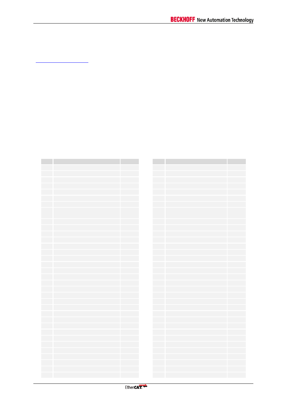
Table 8: Pin Overview
Pin
Pin name
Dir.
Pin
Pin name
Dir.
A1
PDI[27]/RX_DV(3)/EBUS(3)-RX-
BD/LI-
D7
GND
Core
A2
PDI[26]/TX_ENA(3)/EBUS(3)-TX+
BD/LO+
D8
Res. [7]
I
A3
PDI[24]/TX_D(3)[1]/EBUS(3)-TX-
BD/LO-
D9
GND
I/O
A4
PDI[22]/TX_D(3)[3]
BD
D10
V
CC I/O
A5
PDI[20]/RX_D(3)[3]
BD
D11
PDI[1]
BD
A6
PDI[18]/RX_D(3)[0]
BD
D12
PDI[0]
BD
A7
PDI[16]/RX_ERR(3)
BD
E1
TX_D(2)[1]/EBUS(2)-TX-
O/LO-
A8
PDI[14]
BD
E2
PDI[34]/TX_D(2)[0]/
CTRL_STATUS_MOVE
BD
A9
PDI[12]
BD
E3
LINKACT(2)/P_CONF[2]
BD
A10
PDI[10]
BD
E4
Res. [0]
I
A11
PDI[8]
BD
E9
V
CC I/O
A12
PDI[6]
BD
E10
Res. [3]
I
B1
PDI[29]/RX_D(3)[1]/EBUS(3)-RX+
BD/LI+
E11
SYNC/LATCH[0]
BD
B2
PDI[28]/PERR(3)/TRANS(3)
BD
E12
SYNC/LATCH[1]
BD
B3
PDI[25]/TX_D(3)[0]
BD
F1
TX_ENA(2)/EBUS(2)-TX+
BD/LO+
B4
PDI[23]/TX_D(3)[2]
BD
F2
LINK_MII(2)/CLK25OUT1
BD
B5
PDI[21]/LINK_MII(3)
BD
F3
V
CC I/O
(T0)
B6
PDI[19]/RX_D(3)[2]
BD
F4
Res. [6]
I
B7
PDI[17]/RX_CLK(3)
BD
F9
GND
I/O
B8
PDI[15]
BD
F10
V
CC I/O
B9
PDI[13]
BD
F11
EEPROM_DATA
BD
B10
PDI[9]
BD
F12
OSC_OUT
O
B11
PDI[7]/CPU_CLK
BD
G1
PDI[35]/RX_ERR(2)
BD
B12
PDI[4]
BD
G2
PDI[36]/RX_CLK(2)
BD
C1
PDI[31]/CLK25OUT2
BD
G3
Res. [1]
I
C2
PDI[30]/LINKACT(3)/P_CONF(3)
BD
G4
Res. [2]
I
C3
PERR(2)/TRANS(2)/PHYAD_OFF
BD
G9
GND
PLL
C4
RBIAS
G10
V
CC PLL
C5
V
CC I/O
G11
EEPROM_CLK
BD
C6
V
CC Core
G12
OSC_IN
I
C7
V
CC Core
H1
RX_DV(2)/EBUS(2)-RX-
I/LI-
C8
Res. [4]
I
H2
PDI[37]/RX_D(2)[0]
BD
C9
PDI[11]
BD
H3
TESTMODE
I
C10
PDI[5]
BD
H4
GND
I/O
(T1)