Figure 4-1, Mvme5100 block diagram, Functional description – Artesyn MVME51005E SBC Installation and Use (July 2014) User Manual
Page 68: Pci expansion
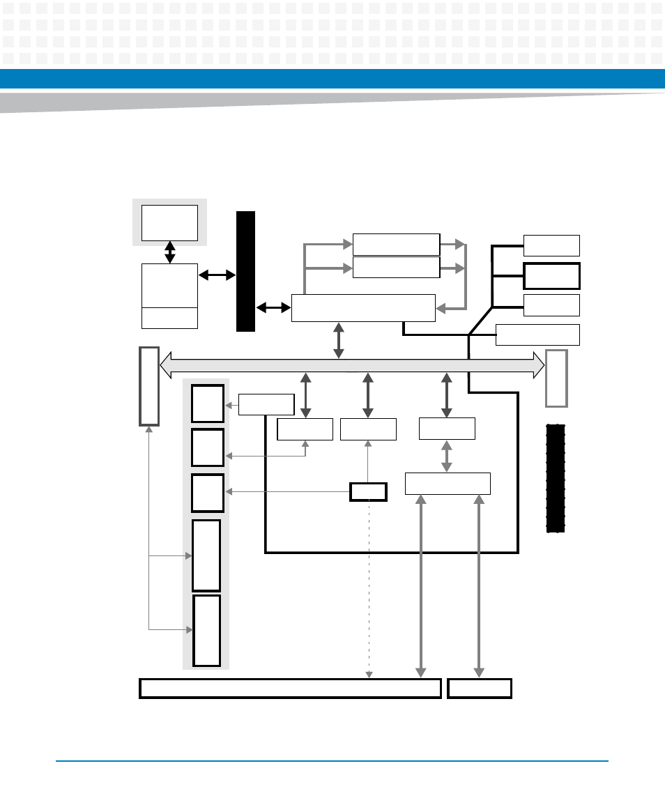
Functional Description
MVME51005E Single Board Computer Installation and Use (6806800A38D)
70
The following diagram illustrates the architecture of the MVME5100 Single Board Computer.
Figure 4-1
MVME5100 Block Diagram
Processor
MPC7410
100
MHz
MPC604
Pr
ocessor
Bus
VME P1
PCI
Expansion
System
Registers
FLASH
1MB to 17MB
Clock
Generator
VME Bridge
Universe 2
Ethernet 1
10/100TX
Buffers
RTC/NVRAM/WD
M48T37V
TL16C550
UART/9pin
Front
Panel
VME P2
RJ45
PMC
Fr
ontI/O
PMC
Fr
ont
I/O
SLot1
Slot2
2,64-bit
PMC
Slots
L2 Cache
1M,2M
Ethernet 2
10/100TX
10/100TX
RJ45
10/100TX
Hawk X-bus
RJ45
DEB
UG
planar
712/761 or PMC
IPMC761
RECEPT
ACLE
Mezzanine SDRAM
32MB to 512MB
SDRAM
32MB to 512MB
HDR
Hawk Asic
System Memory Controller (SMC)
and PCI Host Bridge (PHB)
TL16C550
UART
33MHz 32/64-bit PCI Local Bus
MPC750
See also other documents in the category Artesyn Equipment:
- ARTM-9405 16x10GbE Installation and Use Guide (May 2014) (64 pages)
- ATCA 7370 / ATCA 7370-S Installation and Use (January 2015) (256 pages)
- ATCA 7370 / ATCA 7370-S Installation and Use (September 2014) (254 pages)
- ARTM-831X Installation and Use (June 2014) (346 pages)
- ATCA-7350 - Integrating with Workbench User Guide (September 2014) (34 pages)
- ATCA-7350 Installation and Use (September 2014) (208 pages)
- ATCA-7365-CE Installation and Use (May 2014) (306 pages)
- ATCA-7365-CE Installation and Use (Jan 2015) (300 pages)
- ATCA-7365-CE Installation and Use (May 2014) (294 pages)
- ATCA-7368 Installation and Use (June 2014) (222 pages)
- ATCA-7475 Installation and Use (October 2014) (284 pages)
- ATCA-7480 Installation and Use (April 2015) (330 pages)
- ATCA-8330 Installation and Use (April 2015) (236 pages)
- ATCA-8320 Installation and Use (May 2014) (456 pages)
- ATCA-9305 User's Manual (May 2014) (270 pages)
- ATCA-9405 Installation and Use (October 2014) (168 pages)
- ATCA-F120 Installation and Use (August 2014) (122 pages)
- ATCA-F140 Installation and Use (September 2014) (138 pages)
- ATCA-MF106 Installation and Use (September 2014) (86 pages)
- Centellis-4440/AXP1440 Installation and Use (September 2014) (208 pages)
- Centellis 4410 (AXP-1410) Installation and Use (July 2014) (202 pages)
- Centellis 2100 Release 3.0 Installation and Use (March 2015) (192 pages)
- Centellis 2100 Release 3.0 Installation and Use (March 2015) (176 pages)
- Centellis 2000 User Card-10GE Installation and Use (May 2014) (54 pages)
- Centellis 2000 User Card-10GE with Telco Alarm Installation and Use (May 2014) (60 pages)
- COMX-CAR-210 Installation and Use (August 2014) (76 pages)
- COMX-P1022 Installation and Use (July 2014) (84 pages)
- COMX-P2020 Installation and Use (February 2015) (100 pages)
- COMX-CORE Series Installation and Use (August 2014) (128 pages)
- COMX-P2020 Installation and Use (July 2014) (100 pages)
- COMX-P4080-2G-ENP2 Installation and Use (August 2014) (70 pages)
- COMX-P4080 Installation and Use (August 2014) (126 pages)
- COMX-P40x0 ENP2 Installation and Use (August 2014) (130 pages)
- COMX-P40x0 ENP2 Installation and Use (January 2015) (140 pages)
- iVPX7225 RTM Installation and Use (April 2015) (56 pages)
- MITX-430/MITX-440-DVI-2E Installation and Use (August 2014) (118 pages)
- CPCI-6200 Installation and Use (May 2015) (234 pages)
- SCP-MITX-CORE-820-SM Installation and Use (August 2014) (132 pages)
- iVPX7225 Installation and Use (April 2015) (168 pages)
- MVME2502 Installation and Use (August 2014) (150 pages)
- MVME2502 Installation and Use (December 2014) (166 pages)
- MVME2500 VxWorks 6.8 AMP User Guide (August 2014) (40 pages)
- MVME2500 VxWorks 6.8 User Guide (April 2014) (44 pages)
- MVME3100 Single Board Computer Installation and Use (June 2014) (156 pages)
- MVME4100 Single Board Computer Installation and Use (June 2014) (136 pages)