1 default processor memory map, Table 7-1, Default processor memory map – Artesyn MVME51005E SBC Installation and Use (July 2014) User Manual
Page 116: Programming the mvme5100
Programming the MVME5100
MVME51005E Single Board Computer Installation and Use (6806800A38D)
118
7.2.1.1
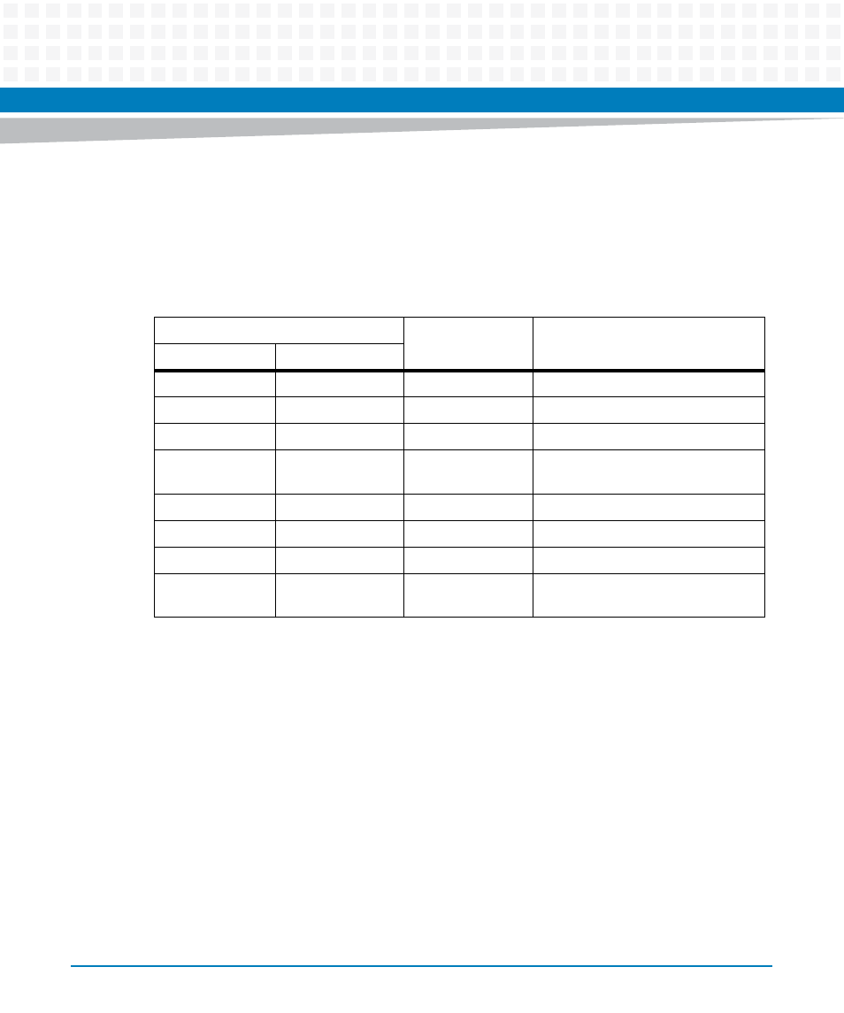
Default Processor Memory Map
The default processor memory map that is valid at power-up or reset remains in effect until
reprogrammed for specific applications.
defines the entire default map ($00000000
to $FFFFFFFF)
Note: The first 1MB of ROM/FLASH Bank A (soldered Flash up to 8MB) appears in this range
after a reset if the rom_b_rv control bit in the SMC’s ROM B Base/Size register is cleared. If the
rom_b_rv control bit is set, this address range maps to ROM/FLASH Bank B (socketed 1MB
Flash).
Table 7-1 Default Processor Memory Map
Processor Address
Size
Definition
Start
End
0000 0000
7FFF FFFF
2GB
Not Mapped
8000 0000
8080 FFFF
8M+64K
Zero-based PCI/ISA I/O Space
8081 0000
FEF7 FFFF
2GB-24MB-576KB
Not Mapped
FEF8 0000
FEF8 FFFF
64KB
System Memory Controller
Registers
FEF9 0000
FEFE FFFF
384KB
Not Mapped
FEFF 0000
FEFF FFFF
64KB
PCI Host Bridge (PHB) Registers
FF00 0000
FFEF FFFF
15MB
Not Mapped
FFF0 0000
FFEF FFFF
1MB
ROM/FLASH Bank A or Bank B (See
Note)
- ARTM-9405 16x10GbE Installation and Use Guide (May 2014) (64 pages)
- ATCA 7370 / ATCA 7370-S Installation and Use (January 2015) (256 pages)
- ATCA 7370 / ATCA 7370-S Installation and Use (September 2014) (254 pages)
- ARTM-831X Installation and Use (June 2014) (346 pages)
- ATCA-7350 - Integrating with Workbench User Guide (September 2014) (34 pages)
- ATCA-7350 Installation and Use (September 2014) (208 pages)
- ATCA-7365-CE Installation and Use (May 2014) (306 pages)
- ATCA-7365-CE Installation and Use (Jan 2015) (300 pages)
- ATCA-7365-CE Installation and Use (May 2014) (294 pages)
- ATCA-7368 Installation and Use (June 2014) (222 pages)
- ATCA-7475 Installation and Use (October 2014) (284 pages)
- ATCA-7480 Installation and Use (April 2015) (330 pages)
- ATCA-8330 Installation and Use (April 2015) (236 pages)
- ATCA-8320 Installation and Use (May 2014) (456 pages)
- ATCA-9305 User's Manual (May 2014) (270 pages)
- ATCA-9405 Installation and Use (October 2014) (168 pages)
- ATCA-F120 Installation and Use (August 2014) (122 pages)
- ATCA-F140 Installation and Use (September 2014) (138 pages)
- ATCA-MF106 Installation and Use (September 2014) (86 pages)
- Centellis-4440/AXP1440 Installation and Use (September 2014) (208 pages)
- Centellis 4410 (AXP-1410) Installation and Use (July 2014) (202 pages)
- Centellis 2100 Release 3.0 Installation and Use (March 2015) (192 pages)
- Centellis 2100 Release 3.0 Installation and Use (March 2015) (176 pages)
- Centellis 2000 User Card-10GE Installation and Use (May 2014) (54 pages)
- Centellis 2000 User Card-10GE with Telco Alarm Installation and Use (May 2014) (60 pages)
- COMX-CAR-210 Installation and Use (August 2014) (76 pages)
- COMX-P1022 Installation and Use (July 2014) (84 pages)
- COMX-P2020 Installation and Use (February 2015) (100 pages)
- COMX-CORE Series Installation and Use (August 2014) (128 pages)
- COMX-P2020 Installation and Use (July 2014) (100 pages)
- COMX-P4080-2G-ENP2 Installation and Use (August 2014) (70 pages)
- COMX-P4080 Installation and Use (August 2014) (126 pages)
- COMX-P40x0 ENP2 Installation and Use (August 2014) (130 pages)
- COMX-P40x0 ENP2 Installation and Use (January 2015) (140 pages)
- iVPX7225 RTM Installation and Use (April 2015) (56 pages)
- MITX-430/MITX-440-DVI-2E Installation and Use (August 2014) (118 pages)
- CPCI-6200 Installation and Use (May 2015) (234 pages)
- SCP-MITX-CORE-820-SM Installation and Use (August 2014) (132 pages)
- iVPX7225 Installation and Use (April 2015) (168 pages)
- MVME2502 Installation and Use (August 2014) (150 pages)
- MVME2502 Installation and Use (December 2014) (166 pages)
- MVME2500 VxWorks 6.8 AMP User Guide (August 2014) (40 pages)
- MVME2500 VxWorks 6.8 User Guide (April 2014) (44 pages)
- MVME3100 Single Board Computer Installation and Use (June 2014) (156 pages)
- MVME4100 Single Board Computer Installation and Use (June 2014) (136 pages)