2 processor memory map, Table 7-2, Suggested chrp memory map – Artesyn MVME51005E SBC Installation and Use (July 2014) User Manual
Page 117: Programming the mvme5100
Programming the MVME5100
MVME51005E Single Board Computer Installation and Use (6806800A38D)
119
7.2.1.2
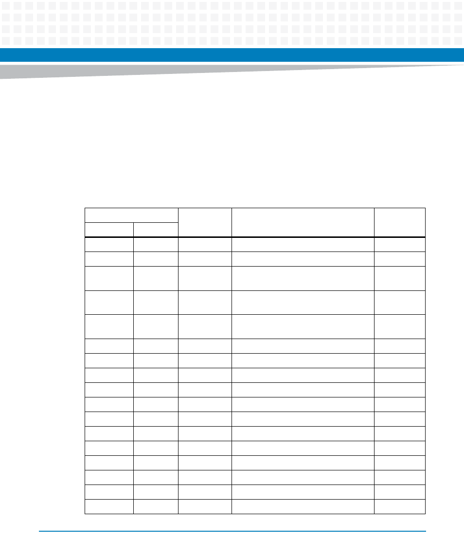
Processor Memory Map
The following table describes a suggested CHRP Memory Map from the point of view of the
processor. This memory map is an alternative to the PREP memory map. Note: in all
recommended CHRP maps, the beginning of PCI Memory Space is determined by the end of
DRAM rounded up to the nearest 256MB-boundary as required by CHRP. For example, if
memory was 1G on the baseboard and 192MB on a mezzanine, the beginning of PCI memory
would be rounded up to address 0x50000000 (1G + 256M).
Table 7-2 Suggested CHRP Memory Map
Processor Address
Size
Definition
Notes
Start
End
0000 0000
top_dram
dram_size
System Memory (onboard DRAM)
1
top_dram
8000 0000 variable
PCI Memory Space
1, 5
8081 0000
9FFF FFFF
512MB
A32/D32 space mapped to VMEbus
starting address of 0100 0000
A000 0000
A1FF FFFF
32MB
A24/D16 space mapped to VMEbus
starting address of F000 0000
AFFF 0000
AFFF FFFF
64KB
A16/D16 space mapped to VMEbus
starting address of FFFF 0000
F400 0000
F7FF FFFF
64MB
FLASH Bank A (optional)
1, 2
FC00 0000
FDFF FFFF
32MB
Reserved
F800 0000
FBFF FFFF
64MB
FLASH Bank B (optional)
1, 2
FE00 0000
FE7F FFFF
8MB
PCI/ISA I/O Space
1
FE80 0000
FEF7 FFFF
7.5MB
Reserved
FEF8 0000
FEF8 FFFF
64KB
System Memory Controller Registers
FEF9 0000
FEFE FFFF
384KB
Reserved
FEFF 0000
FEFF FFFF
64KB
Processor Host Bridge Registers
FF00 0000
FF7F FFFF
8MB
FLASH Bank A (preferred)
1, 2
FF80 0000
FF8F FFFF
1MB
FLASH Bank B (preferred)
1, 2
FF90 0000
FFEF FFFF
6MB
Reserved
FFF0 0000
FFEF FFFF
1MB
Boot ROM
3