Figure 4-5, Base channel block diagram, Functional description – Artesyn ATCA-F125 Installation and Use Guide (April 2014) User Manual
Page 76
Functional Description
ATCA-F125 (6873M Artwork) Installation and Use (6806800J94J)
76
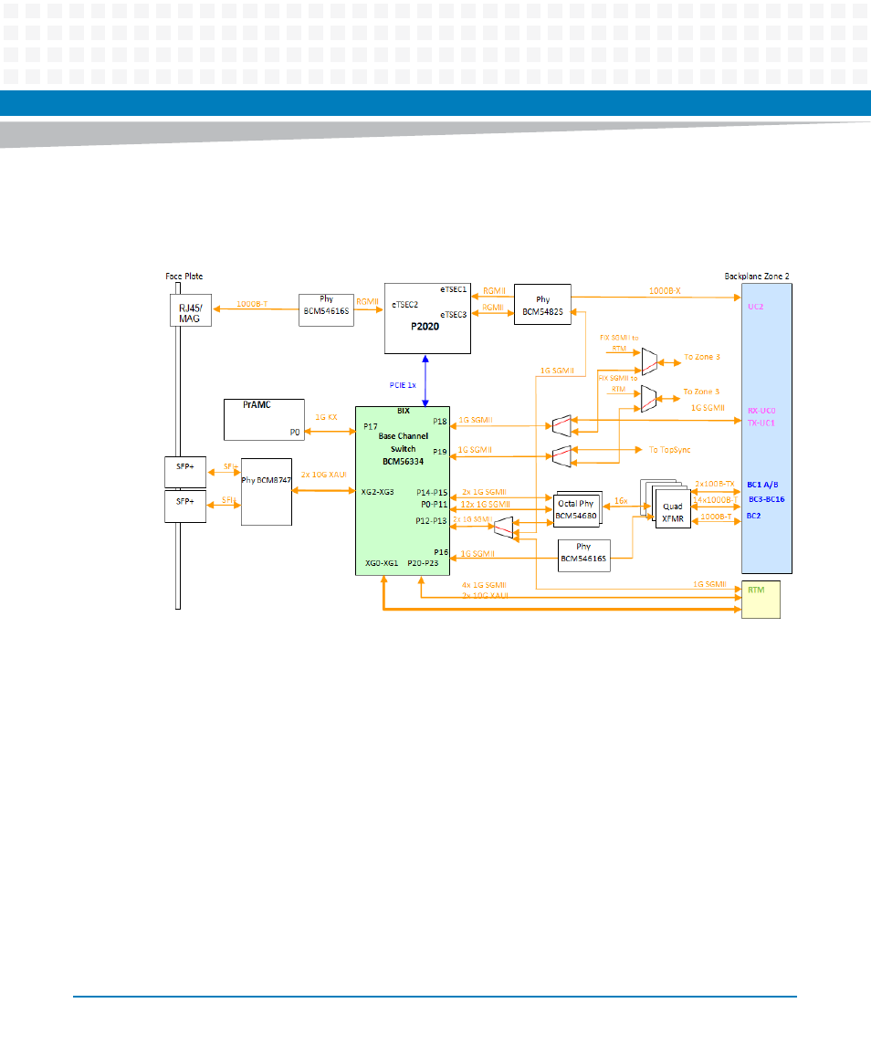
access to the BCM56334 switch traffic. A block diagram of the base channel interconnect is
shown in
.
Some of the 1GbE SGMII ports from the BCM56334 have the option of being routed through
muxes to different destinations as seen in the block diagram above (for example, to ToPSync or
RTM). The select pins for these mux/demux switches are located in the FGPA to route the SGMII
ports to the desired destination. FPGA registers can be accessed through two different
methods:
1. Through the P2020 local bus interface, the service processor can program registers in the
FPGA
2. Through the IPMI controller private I2C bus, the IPMC controller can set the various mux
select before enabling reset on the remainder to the payload.
Figure 4-5
Base Channel Block Diagram