Ft router 5000 – Echelon LonWorks Router User Manual
Page 98
transceiver PCB are the clamping diodes (D6-D9) for the transceiver’s receive
signals.
FT Router 5000
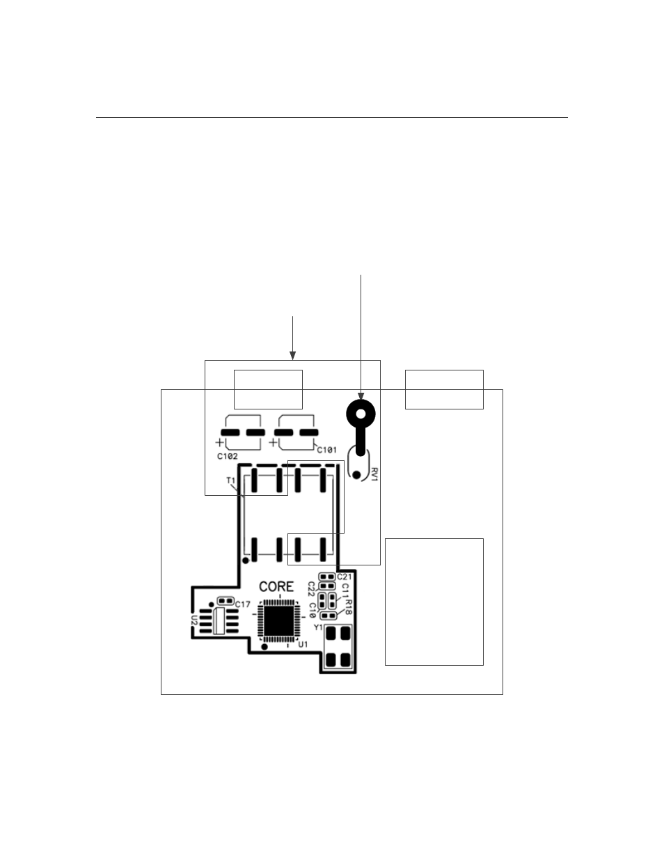
Figure 43 shows a portion of the top layer of a 4-layer PCB layout for an FT
Router 5000 half-router, including the FT-X3 Communications Transformer and
the other building blocks of a PCB design.
See Chapters 3 and 4 of the Series 5000 Chip Data Book for additional
information about PCB layout and electromagnetic compatibility (EMC) design
guidelines for a Series 5000 Chip, including the FT Router 5000.
Network
Connector
Power Supply
Circuitry
Power Supply
Connector
Center of
Star Ground
EMC
Keepout
Area
Figure 43. Example PCB Layout for an FT Router 5000
In the figure, the area marked CORE represents the essential circuitry for the FT
Router 5000, the FT-X3 Communications Transformer, the router chip’s serial
EEPROM memory chip, its crystal, and associated capacitors and resistors. The
figure does not show I/O or other connections to the other side of the router.
88
LONWORKS Router Design Issues