Example router 5000 schematics – Echelon LonWorks Router User Manual
Page 81
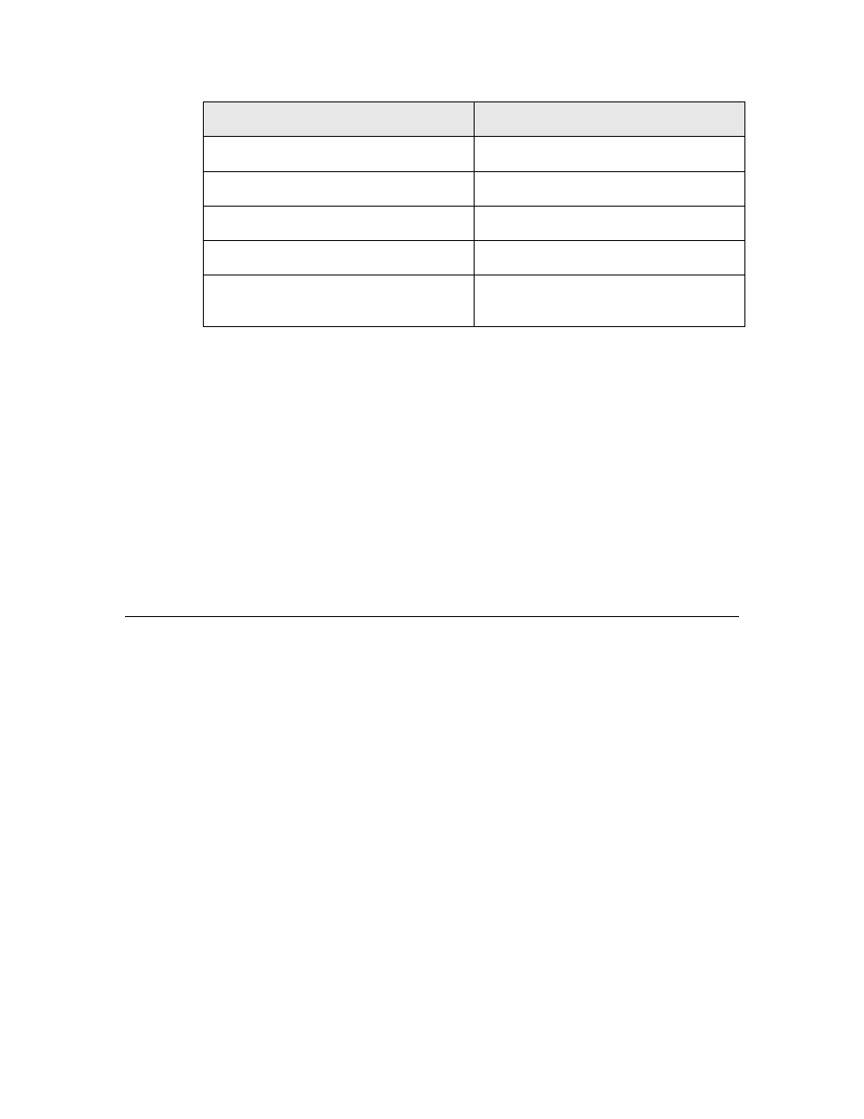
Designator
Value
R2
1 MΩ
R3
200 Ω
U1
TDA3663 (or similar LDO regulator)
U2
74AHCT1G126
U3
74AHCT1G04 (or a 74AHCT1G126
with OE tied high)
Important: Because the Router 5000 XOUT pin drives the LPT-11 CLK signal,
the value of C2 does not match the value of C1. The value for C2 is specified as
30 pF based on an input capacitance for the buffer/line driver of 3 pF at 25 ºC (so
that the total capacitance for the XOUT pin is 33 pF). For the 74AHCT1G126
part, input capacitance can vary over temperature, up to 10 pF. If your device is
likely to experience extreme temperatures, consider changing the value of C2 to
27 pF to allow for the change in capacitance over temperature.
See the L
ON
W
ORKS
LPT-11 Link Power Transceiver User’s Guide for additional
information about selecting appropriate parts for capacitors C3 and C5 and for
inductor L1.
See the L
ON
W
ORKS
LPT-11 Link Power Transceiver User’s Guide for PCB layout
guidelines for the LPT-11 transceiver; see PCB Layout Guidelines and the Series
5000 Chip Data Book for PCB layout guidelines for the Router 5000.
Example Router 5000 Schematics
Figure 36 a sample core schematic for two Router 5000 half routers. This core
schematic could apply to any Router 5000 router. Figure 37 shows a sample
schematic for the transceivers used by each router half; in this example, TP/XF-
1250 and EIA-485. The transceiver schematics also include the RX and TX
activity indicator circuits described in Network Activity Indicator – Router 5000.
L
ON
W
ORKS
Router User’s Guide
71