Echelon LonWorks Router User Manual
Page 43
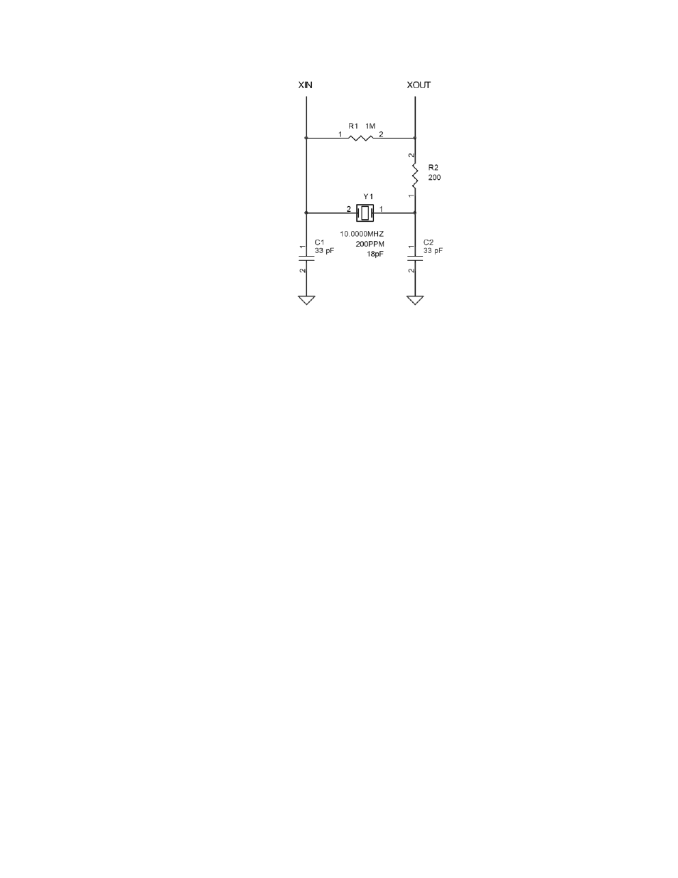
Figure 13. Series 5000 Chip Clock Generator Circuit
To ensure proper oscillator startup, the equivalent series resistance specification
for the crystal should be ≤50 Ω, and the crystal shunt capacitance should be no
greater than 7 pF.
Using a 33 pF capacitor for C2 (in Figure 13), the Series 5000 router chip’s
XOUT pin cannot be used to drive an external CMOS load. However, if you
maintain the required capacitance for the XOUT pin, you can drive an external
clock, for example, for another Series 5000 half-router.
If your Series 5000 router device requires a common clock signal for both router
halves, you can adjust the value for C2 (in Figure 13), add a buffer, and leave
the B Side XOUT unconnected, as shown in Figure 14.Clock traces should be
kept short (≤2 cm, ≤0.8 inch). Keep the crystal circuit close to the Router 5000
chips and isolated from communications lines. In addition, a logic ground guard
must be added for the clock trace to minimize clock noise and to help keep EMI
levels low. However, this ground guard should not be used as a ground source for
digital circuitry.
In addition, the connection between A Side XOUT pin and the B Side XIN pin
includes standard (inverting or non-inverting) bus buffer/line driver.
Important: Because the Series 5000 router A Side XOUT pin drives an input
buffer, the values of the external capacitors are not equal. The value for A Side
XOUT is specified as 30 pF based on an internal input capacitance of 4.5 pF of
the XIN/XOUT pins and internal input capacitance for the buffer/line driver of 3
pF at 25 ºC (so that the total capacitance for the A Side XOUT pin is 33 pF). For
some bus buffer/line drivers, input capacitance can vary over temperature, up to
10 pF. If your device is likely to experience extreme temperatures, consider
changing the value for the A Side XOUT capacitor to 27 pF to allow for the
change in capacitance over temperature.
L
ON
W
ORKS
Router User’s Guide
33