Control pin functions and applications, Control functions and output considerations – Vicor Micro Family of DC-DC Converter User Manual
Page 9
Design Guide & Applications Manual
For Maxi, Mini, Micro Family DC-DC Converters and Configurable Power Supplies
Maxi, Mini, Micro Design Guide
Rev 4.9
vicorpower.com
Page 8 of 88
Apps. Eng. 800 927.9474
800 735.6200
2. Control Pin Functions and Applications
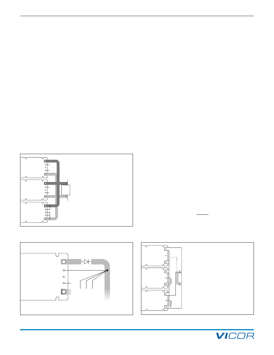
Parallel Operation (PR Pin). The PR pin supports paral-
leling for increased power with N+1or N+M redundancy.
Modules of the same part number will current share if all
PR pins are suitably interfaced. Figures 2–9 and 2–10
show connections for the Maxi and Mini modules; Figure
2–11 shows connections for Micro array. Applications
containing two or more Micro modules must define a
designated master (talker) by stagger trimming the output
voltage of each subsequent module down by at least 2%,
or setting the remaining Micro modules in the system as
designated listeners by connecting the SC pin to the
negative output pin.
PR Pin Considerations. When paralleling modules, it is
important that the PR signal is communicated to all
modules within the parallel array. Modules that do not
receive a PR pulse in a parallel array will not current share
and may be damaged by running in an over-power
condition.
All modules in an array must be of the same part
number.Series connection of outputs is accomplished
without connecting the PR pins and allowing each module
to regulate its own output voltage. Since the same current
passes through the output of each module with the series
connection, power sharing is inherent. Series connection
of inputs requires special precautions, please contact
Applications Engineering for assistance.
Array Output Overvoltage Protection (OVP). In order
to maintain the highest possible uptime of a parallel array
the converters use an output overvoltage protection
system (OVP) that is highly resistant to false tripping. For
the converter to shut down due to an OVP condition two
conditions must be satisfied (logical AND);
1. The voltage at the output terminals must be greater
than the OVP set point.
2. The secondary control IC within the converter must be
requesting a power conversion cycle from the internal
primary control IC.
By using this logic, false tripping of individual converters
due to externally induced OVP conditions such as load
dumps or, being driven by an external voltage source at
the output terminals is minimized.
Modules connected in a parallel array rely on the active
master module for OVP of the entire array. Modules acting
as boosters (slaves) in the array are receiving external
requests for power conversion cycles (PR pulse) and will
not shut down from an OVP condition. Therefore it is
imperative that the + and -Output pins of modules
connected in a parallel array never be allowed to become
open circuited from the output bus. An open circuit at the
output terminals will result in terminal voltages far in
excess of the normal rating causing permanent damage
to the module and possible hazardous conditions.
Module 2
Module 1
Module N+1
+OUT
+S
SC
–S
–OUT
Load
+S
–S
+S
–S
+S
–S
+OUT
+S
SC
–S
–OUT
+OUT
+S
SC
–S
–OUT
+OUT
+S
SC
–S
–OUT
+Sense from
other modules
in the array
+OUT
SC
–OUT
L
O
A
D
Plane
Ground
Plane
Module #1
Designated
Master
Module #2
trimmed
down 2 %
Module #3
trimmed
down 4 %
+OUT
SC
–OUT
+OUT
SC
–OUT
• The +Out and –Out power buses
should be designed to minimize and
balance parasitic impedance from
each module output to the load.
• The +Sense pins should be tied to the same
point on the +Out power bus; (Figure 2-10)
the –Sense pins should be tied to the same
point on the –Out power bus.
• At the discretion of the power system
designer, a subset of all modules within
an array may be configured as slaves
by shorting SC to –S.
• ORing diodes may be inserted in series
with the +OUT pins of each module to
provide module output fault tolerance.
• The +Out and –Out power buses should
be designed to minimize and balance
parasitic impedance from each module
output to the load.
• At the discretion of the power system
designer, a subset of all modules within
an array may be configured as slaves
by shorting SC to –Out.
• Do not use output ORing diodes
with parallel arrays of the Micro.
CONTROL FUNCTIONS AND OUTPUT CONSIDERATIONS
Figure 2–9 — N+1 module array output connections (Maxi and Mini)
Figure 2–10 — ORing diodes connections (Maxi and Mini)
Figure 2–11 — Parallel module array output connections (Micro)