Control pin functions and applications, Parallel operation considerations – Vicor Micro Family of DC-DC Converter User Manual
Page 8
Design Guide & Applications Manual
For Maxi, Mini, Micro Family DC-DC Converters and Configurable Power Supplies
Maxi, Mini, Micro Design Guide
Rev 4.9
vicorpower.com
Page 7 of 88
Apps. Eng. 800 927.9474
800 735.6200
2. Control Pin Functions and Applications
Care must be taken to avoid introducing interfering signals
(noise) onto the parallel bus that may prevent proper load
sharing between modules, instability, or module failure.
One possible source of interference is input ripple current
conducted via the + and –Input power pins. The PR signal
and DC power input share a common return, which is the
–Input pin. Steps should be taken to decouple AC compo-
nents of input current from the parallel bus. The input to
each converter (designated as + and – pins on the input
side of the module) should be bypassed locally with a
0.2 µF ceramic or film capacitor. This provides a shunt
path for high frequency input ripple current. A Y-rated
4,700 pF capacitor should be connected between both
the + and –Input pins and baseplate of each module, thus
creating a shunt path for common-mode components of
current. Attention to the PC board artwork should minimize
the parasitic impedance between –Input pins of parallel
modules to ensure that all PR pins are referenced to the
same potential, or use a transformer coupled interface.
Modules should be placed physically close to each other
and wide copper traces (0.75 in./19 mm, 2 oz. copper)
should be used to connect power input pins. A dedicated
layer of copper is the ideal solution.
Some applications require physical separation of paralleled
modules on different boards, and / or input power from
separate sources. For applications using separate sources,
please refer to the “Hot-Swap Capability Eliminates
Downtime” application note on Vicor’s website. In these
cases, transformer coupling of the PR signal, per Figure 2–8,
is required to prevent inter-module common-mode noise
from interfering with the sync pulse transmission. High-
speed buffering may be required with large arrays or if the
distance between modules is greater than a few inches.
This is due to the fact that all modules, except the one
that’s talking, are in the listening mode. Each listener
presents a load to the master (talker), which is approxi-
mately 500
Ω shunted by 30 pF capacitance. Long leads
for the interconnection introduce losses and parasitic
reactance on the bus, which can attenuate and distort the
sync pulse signal. The bandwidth of the bus must be at
least 60 MHz and the signal attenuation less than 2 dB.
In most cases, transformer coupling without buffering is
adequate. Many applications may benefit from the addition
of Z1, in series with the PR Pin of each converter. A low Q 33 Ω
@ 100 Mhz ferrite bead or a 5 - 15 Ohm resistor may be
used to improve the PR signal waveform. Although this is
not a requirement, it can be very helpful during the debug
stage of large converter arrays to help improve the PR
pulse wave shape and reduce reflections. Again, careful
attention must be given to layout considerations. When
the outputs of two or more converters are connected in a
parallel array to increase system power the converters
should be “group enabled” to ensure that all the convert-
ers start at the same time. The PC pins of all converters in
the array should be controlled by an external circuit which
will enable the converters once the input voltage is within
the normal operating range. Please consult with
for additional information.
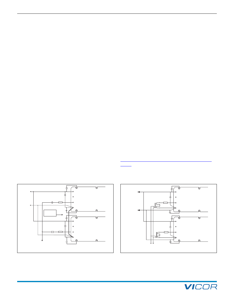
Figure 2–7 — AC coupled single-wire interface
Figure 2–8 — Transformer-coupled interface
+IN
PC
PR
–IN
+IN
PC
PR
–IN
Module 2
Module 1
+
Parallel
Bus
–
0.2 µF
0.001 µF
0.2 µF
0.001 µF
Low inductance
ground plane
or bus
4.7 nF
4.7 nF
4.7 nF
4.7 nF
Z1*
Z1*
+IN
PC
PR
–IN
+IN
PC
PR
–IN
Module 2
Module 1
T1
T2
+
–
0.2 µF
0.2 µF
Parallel
Bus
4.7 nF
4.7 nF
4.7 nF
4.7 nF
Z1
*
Z1
*
PARALLEL OPERATION CONSIDERATIONS