Output ripple attenuator module (microram) – Vicor Micro Family of DC-DC Converter User Manual
Page 58
Design Guide & Applications Manual
For Maxi, Mini, Micro Family DC-DC Converters and Configurable Power Supplies
Maxi, Mini, Micro Design Guide
Rev 4.9
vicorpower.com
Page 57 of 88
Apps. Eng. 800 927.9474
800 735.6200
12. Output Ripple Attenuator Module (MicroRAM)
The SC or trim-up function can be used when remote
sensing is not available on the source converter or is not
desirable. It is specifically designed for converters with a
1.23 V reference and a 1 k
Ω input impedance like Vicor
Maxi, Mini, Micro converters. In comparison to remote
sensing, the SC configuration will have an error in the
load voltage versus load current. It will be proportional to
the output current and the resistance of the load path
from the output of the MicroRAM to the load.
The ORing feature prevents current flowing from the
output of the MicroRAM back through its input terminal
in a redundant system configuration in the event that a
converter output fails. When the converter output
supplying the MicroRAM droops below the ORed output
voltage potential of the redundant system, the input of
the MicroRAM is isolated from it’s output. Less than
50 mA will flow out of the input terminal of the MicroRAM
over the full range of input voltage under this condition.
Load capacitance can affect the overall phase margin of
the MicroRAM active loop as well as the phase margin
of the converter loop. The distributed variables such as
inductance of the load path, the capacitor type and
value as well as its ESR and ESL also affect transient capa-
bility at the load. The following guidelines should
be considered when point-of-load capacitance is used
with the MicroRAM in order to maintain a minimum of
30 degrees of phase margin.
1. Using ceramic load capacitance with <1 m
Ω
ESR and <1 nH ESL:
a. 20 µF to 200 µF requires 20 nH of trace / wire
load path inductance
b. 200 µF to 1,000 µF requires 60 nH of trace / wire
load path inductance
2. For the case where load capacitance is connected
directly to the output of the MicroRAM, i.e. no trace
inductance, and the ESR is >1 m
Ω:
a. 20 µF to 200 µF load capacitance needs an ESL
of >50 nH
b. 200 µF to 1,000 µF load capacitance needs an
ESL of >5 nH
3. Adding low ESR capacitance directly at the output
terminals of MicroRAM is not recommended and may
cause stability problems.
4. In practice, the distributed board or wire inductance
at a load or on a load board will be sufficient to
isolate the output of the MicroRAM from any load
capacitance and minimize any appreciable effect on
phase margin.
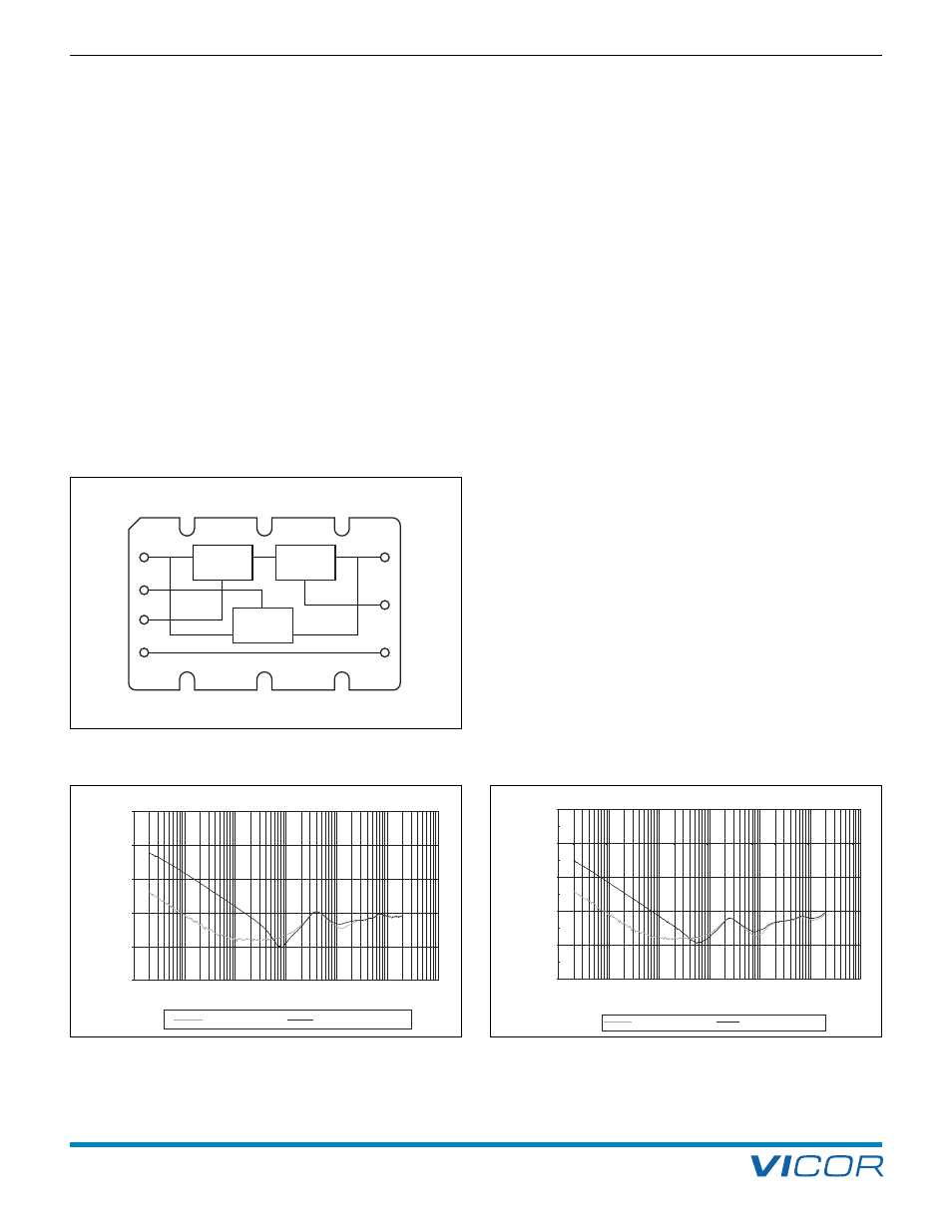
+Out
Vref
–Out
+In
SC
C
TRAN
–In
Passive
Block
Active
Block
SC
Control
Figure 12-2 — MicroRAM block diagram
Ripple Attenuation @ 28 V (Room Temp.)
-80.00
-60.00
-40.00
-20.00
0.00
20.00
10
100
1,000
10,000
100,000
1,000,000 10,000,000
Freq. (Hz)
G
a
in
(
d
B
)
10 A, 100 uF Vref
10 A, No Vref Cap
Figure 12–3a — The small signal attenuation performance as
measured on a network analyzer with a typical module at 28 V and
10 A output. The low frequency attenuation can be enhanced by
connecting a 100 µF capacitor, C
HR
, to the V
REF
pin as shown in
Figures 12–1 and 12–2.
Ripple Attenuation @ 5 V (Room Temp.)
-80.00
-60.00
-40.00
-20.00
0.00
20.00
10
100
1,000
10,000
100,000
1,000,000
10,000,000
Freq. (Hz)
G
a
in
(
d
B
)
10 A, 100 uF Vref
10 A, No Vref Cap
Figure 12–3b — The small signal attenuation performance as
measured on a network analyzer with a typical module at 5 V and
10 A. The low frequency attenuation can be enhanced by connect-
ing a 100 µF capacitor, C
HR
, to the V
REF
pin as shown in Figures
12–1 and 12–2.