Design requirements – Vicor Micro Family of DC-DC Converter User Manual
Page 17
Design Guide & Applications Manual
For Maxi, Mini, Micro Family DC-DC Converters and Configurable Power Supplies
Maxi, Mini, Micro Design Guide
Rev 4.9
vicorpower.com
Page 16 of 88
Apps. Eng. 800 927.9474
800 735.6200
3. Design Requirements
MAXIMUM OUTPUT CAPACITANCE
In general, adding external capacitance to the Maxi, Mini,
and Micro’s output is not required. However, it is often
common practice with power supply designs to add external
capacitance to the converter output for attenuation of
output ripple and / or improving dynamic load performance.
The Maxi, Mini, Micro converters typically have a faster
response to dynamic loads than other power solutions;
hence, external capacitors may not be necessary. In addition,
the output ripple and noise specification listed on the data
sheet may be acceptable for many applications.
A general equation for determining the maximum recom-
mended output capacitance is as follows:
P
out
(400x10
-6
)
C
(farad)
=
V
out
V
out
where: P
out
is the output power of the converter
V
out
is the nominal output voltage of the converter
The capacitance value is not the absolute maximum value,
but the value for which general application of the converter
can be deemed appropriate. Testing will be required to
ensure that the module is stable if this value is exceeded.
Approximately 10X the value calculated will cause the
converter to go into current limit at turn-on.
CAUTION: If exceeding this value, it is recommended
that Vicor Applications Engineering be consulted.
ABSOLUTE MAXIMUM RATINGS
Please consult the latest module data sheets available on
the Vicor website for maximum ratings concerning pin-to-
pin voltages, isolation, temperature, and mechanical ratings.
GROUNDING OF BASEPLATE AND REFERENCING
OF INPUT AND OUTPUT TERMINALS
The baseplate of the converter should always be connected
to earth ground. If for any reason this is not possible in
your application please consult with Vicor Applications
Engineering for acceptable alternatives for your application.
The input and output leads of the converter should be
referenced to the baseplate at some point to avoid stray
voltages. For offline applications the input leads are often
referenced to earth ground at the AC source ahead of the
bridge rectifier. Either + or –Output terminal may be
referenced to earth ground and the baseplate. “Floating”
inputs or outputs should at a minimum have a high-
resistance divider to bleed off stray charges to avoid
damage to the insulation system.
HIGH FREQUENCY BYPASSING
All Vicor converters must be bypassed for proper operation.
(Figure 3–2) The minimum complement of high-frequency
bypass capacitors must consist of the following:
•
0.2 µF ceramic or film type connected between
+In and –In.
•
4.7 nF Y-capacitor between +In and baseplate
and –In and baseplate.
•
10 nF ceramic or film capacitor between +Out and
baseplate and –Out and baseplate.
All applications utilizing Maxi, Mini, Micro converters
should be properly bypassed, even if no EMC standards
need to be met. Bypass Vin and Vout pins to each module
baseplate as shown in Figure 3–2. Lead length should
be as short as possible. Recommended values vary
depending on the front end, if any, that is used with the
modules, and are indicated on the appropriate data sheet
or application note. In most applications, C1 is a 4,700 pF
Y-capacitor (Vicor P/N 01000) carrying the appropriate
safety agency approval; C2 is a 4,700 pF Y-capacitor (Vicor
P/N 01000) or a 0.01 µF ceramic capacitor rated at 500 V.
In PC board applications, each of these components is
typically small enough to fit under the module baseplate
flange. For PCB mounting of the module. Please refer to
Figures 3–3 and 3–4.
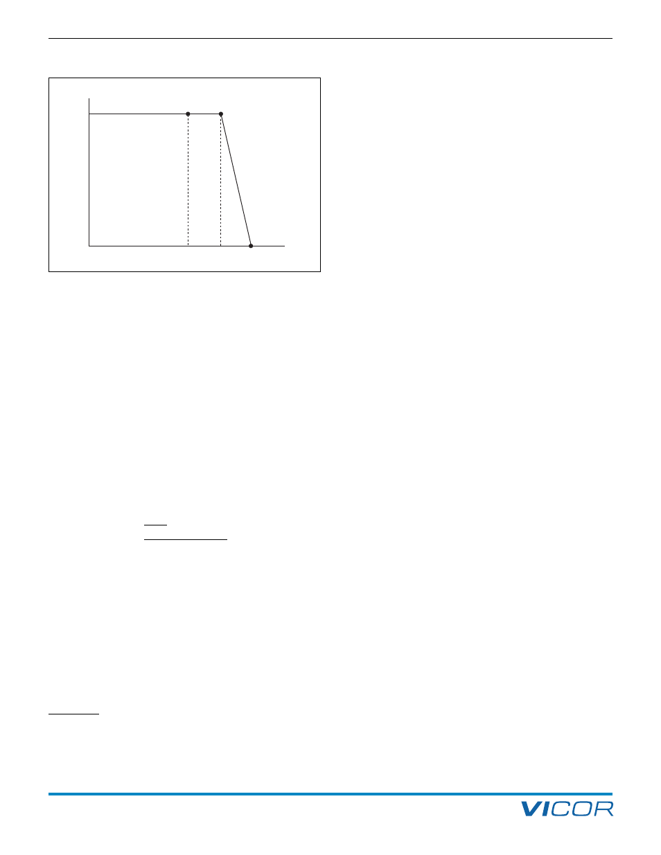
Vout
I
KNEE
I
MAX
I
SHORT CIRCUIT
Iout
Figure 3–1 — Typical Maxi, Mini, Micro current limiting