Autoranging rectifier module (arm) – Vicor Micro Family of DC-DC Converter User Manual
Page 32
Design Guide & Applications Manual
For Maxi, Mini, Micro Family DC-DC Converters and Configurable Power Supplies
Maxi, Mini, Micro Design Guide
Rev 4.9
vicorpower.com
Page 31 of 88
Apps. Eng. 800 927.9474
800 735.6200
7. Autoranging Rectifier Module (ARM)
The Autoranging Rectifier Module (ARM) provides an
effective solution for the AC front end of a power supply
designed with Vicor DC-DC converters. This high-perform-
ance power system building block satisfies a broad
spectrum of requirements and agency standards.
The ARM contains all of the power switching and control
circuitry necessary for autoranging rectification, inrush
current limiting, and overvoltage protection. This module
also provides converter enable and status functions for
orderly power up / down control or sequencing. To
complete the AC front-end configuration, the user needs
only to add hold-up capacitors and a suitable input filter
with transient protection.
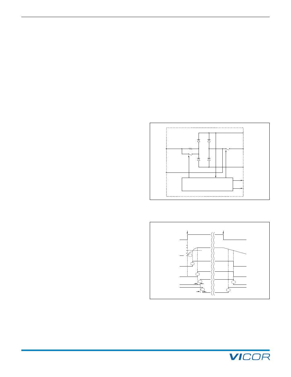
FUNCTIONAL DESCRIPTION (Figure 7–1)
Initial Conditions. The switch that bypasses the inrush
limiting PTC (positive temperature coefficient) thermistor is
open when power is applied, as is the switch that
engages the strap for voltage doubling. In addition, the
downstream DC-DC modules are disabled via the Enable
(EN) line, and Bus OK (BOK) is high.
POWER-UP SEQUENCE (Figure 7–2)
1.1 Upon application of input power, the output bus
capacitors begin to charge. The thermistor limits the
charge current, and the exponential time constant is
determined by the hold-up capacitor value and the
thermistor cold resistance. The slope (dv/dt) of the
capacitor voltage approaches zero as the capacitors
become charged to the peak of the AC line voltage.
2.1 If the bus voltage is less than 200 V as the slope nears
zero, the voltage doubler is activated, and the bus
voltage climbs exponentially to twice the peak line
voltage. If the bus voltage is greater than 200 V, the
doubler is not activated.
3.1 If the bus voltage is greater than 235 V as the slope
approaches zero, the inrush limiting thermistor is
bypassed. Below 235 V, the thermistor is not bypassed.
4.1 The converters are enabled ~150 milliseconds after
the thermistor bypass switch is closed.
5.1 Bus OK is asserted after an additional ~150 millisecond
delay to allow the converter outputs to settle
within specification.
POWER-DOWN SEQUENCE (Figure 7–2)
When input power is turned off or fails, the following
sequence occurs as the bus voltage decays:
1.2 Bus OK is de-asserted when the bus voltage falls
below 205 Vdc (typical).
2.2 The converters are disabled when the bus voltage falls
below 200 Vdc. If power is reapplied after the
converters are disabled, the entire power-up sequence
is repeated. If a momentary power interruption occurs
and power is re-established before the bus reaches the
disable threshold, the power-up sequence is not repeated.
Figure 7–1 — Functional block diagram
Figure 7–2 —Timing diagram: power up / down sequence
Microcontroller
N
L
PTC
Thermistor
+OUT
–OUT
Strap
EN
BOK
Strap
400
300
200
100
0
90–132 V
AC Line
Output
Bus
(Vdc)
Strap
PTC
Thermistor
Bypass
Converter
Enable
Bus OK
~150 ms
Power
Up
Power
Down
Timing Diagram, Power Up/Down Sequence
4.1
1.1
2.1
3.1
5.1
2.2
1.2
~150 ms