Tin lead pins – Vicor Micro Family of DC-DC Converter User Manual
Page 68
Design Guide & Applications Manual
For Maxi, Mini, Micro Family DC-DC Converters and Configurable Power Supplies
Maxi, Mini, Micro Design Guide
Rev 4.9
vicorpower.com
Page 67 of 88
Apps. Eng. 800 927.9474
800 735.6200
14. Recommended Soldering Methods,
Tin Lead Pins, and InMate Sockets
The following chapters contain soldering information for
the following Vicor product families; Maxi, Mini, Micro;
VI-200, VI-J00; VI BRICK
®
, and similar package filters and
front-ends. This document is intended to provide guidance
in utilizing soldering practices to make high-quality con-
nections of Vicor power modules to printed circuit boards.
Some care will be taken to outline appropriate soldering
procedures as well as the evaluation of solder joints in a
manner that enables the customer to ensure that the end
application has an optimal connection to the power
module. Common soldering defects will be examined and
direction will be provided for detecting and handling the
common defects.
Vicor’s manufacturing facilities use the IPC-A-610C
standards as a means of establishing quality solder joints.
It is recommended that manufacturing processes using
Vicor modules refer to these same standards, which can
be found, along with supporting documentation, at
ANALYSIS OF A GOOD SOLDER JOINT
The IPC-A-610C standard requires that solder fill at least
75% of the barrel in order to ensure a solid connection.
Ideally, all connections should have a 100% fill. In order to
accomplish this, the solder applied to both the barrel and
the pin must exhibit a process known as wetting. Wetting
occurs when liquid solder on a surface is heated to the
point that it loses a significant amount of latent surface
tension and evenly coats the surface via capillary action
(both cohesion and adhesion).
During the soldering process wetting can be identified by
an even coating of solder on the barrel and pin. In
addition to coating the surface of barrel and pin, the
solder will gather at the intersection of the two and
produce a trailing fillet along each surface. Once wetting
has occurred, then upon solidification it will bond appro-
priately to both components, producing a quality connec-
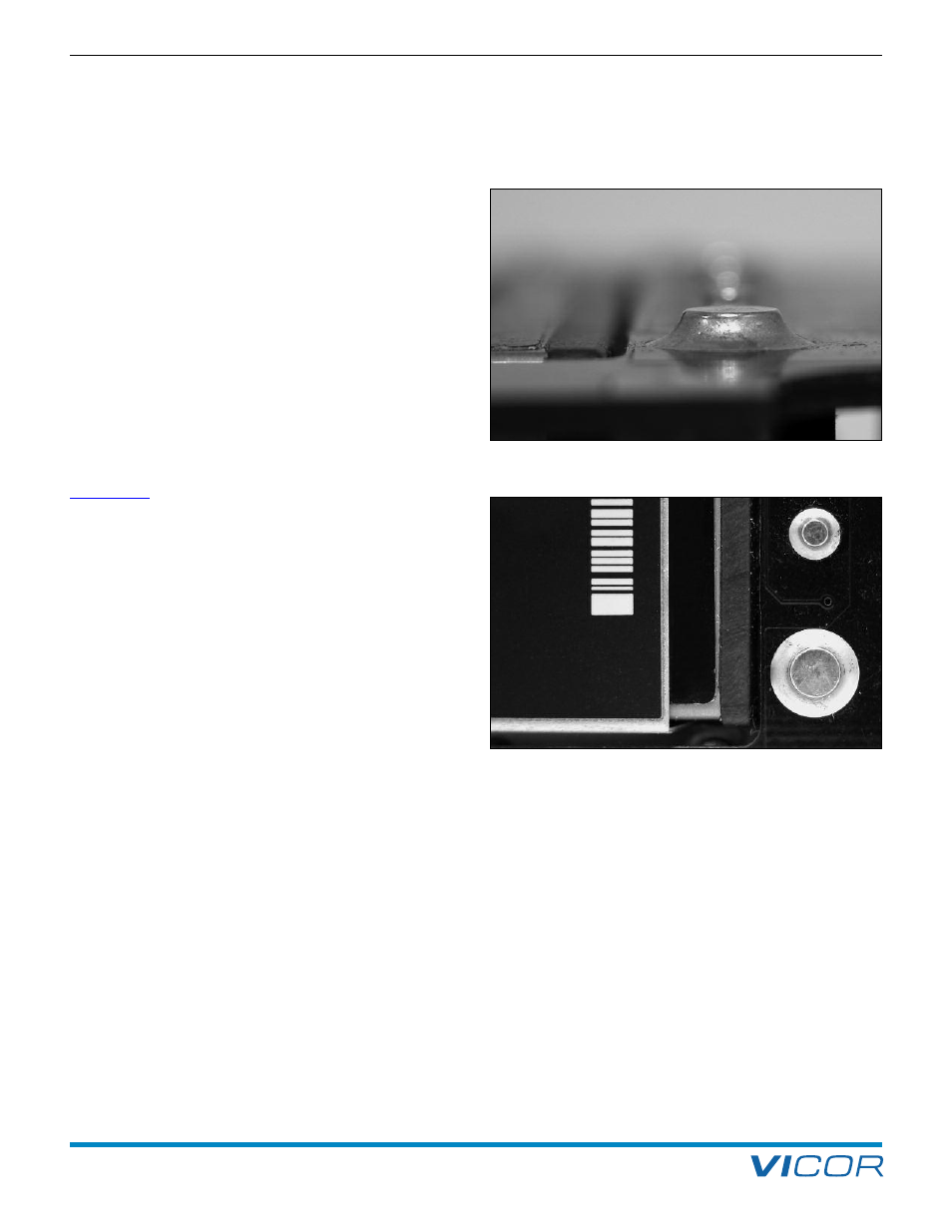
tion. Figure 14–1 shows a side profile of a good solder
joint with a Mini power module. Notice that for both
examples the solder forms a concave meniscus between
pin and barrel. This is an example of a properly formed
fillet and is evidence of good wetting during the soldering
process. The joint between solder and pin as well as
solder and pad should always exhibit a feathered edge. In
Figure 14–1 it can also be seen that the solder covers a
good deal of the surface area of both the pin and the
pad. This is also evidence of good wetting. Notice also
that the solder joint has a smooth surface with a silver
color. This is evidence of good immobilization of the joint
during cooling as well as good cleaning of the board prior
to soldering. All soldering connections should exhibit
similar characteristics regardless of whether they are
soldered by hand or wave soldered.
Figure 14–2 is a top view of the signal and power pin of a
Maxi or Mini module properly soldered to a printed circuit
board. Notice that both the joint and the area around the
joint are clean and free from resin and solder residue. Also
the pad and printed circuit board adjacent to the barrel
are not burnt or discolored and are solidly attached to
each other. In examining a solder joint, be sure that there
is no solder connecting one pad to another. This is known
as a solder bridge and will be discussed further along with
other potential soldering defects.
Figure 14–2 — Maxi / Mini output power pin and Sense pin
Figure 14–1 — Side profile of a Mini module solder joint
OVERVIEW