Autoranging rectifier module (arm), Figure 7–3 — typical arm application, Design guide & applications manual – Vicor Micro Family of DC-DC Converter User Manual
Page 33: Page 32 of 88
Design Guide & Applications Manual
For Maxi, Mini, Micro Family DC-DC Converters and Configurable Power Supplies
Maxi, Mini, Micro Design Guide
Rev 4.9
vicorpower.com
Page 32 of 88
Apps. Eng. 800 927.9474
800 735.6200
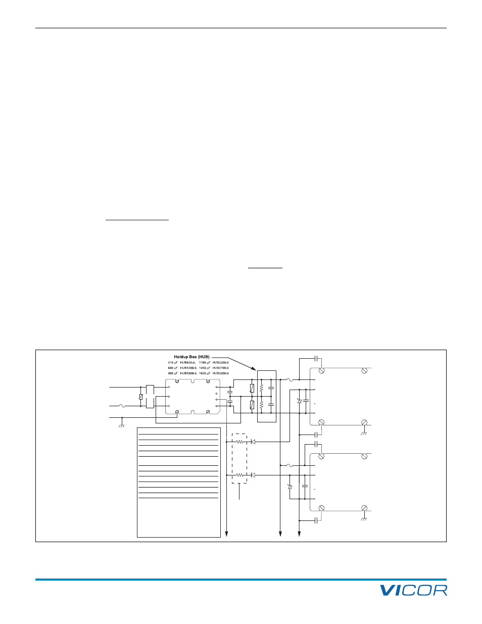
7. Autoranging Rectifier Module (ARM)
OFF-LINE POWER SUPPLY CONFIGURATION
The ARM maintains the DC output bus voltage between
200 and 375 Vdc over the entire universal input range,
this being compatible with the Maxi, Mini, Micro 300 V
input converters as well as VI-260 family and VI-J60 family
DC-DC converters. The ARM automatically switches to the
proper rectification mode (doubled or undoubled) depending
on the input voltage, eliminating the possibility of damage
due to improper line connection. The VI-ARM-x1 is rated at
500 W in the low range (90 –132 Vac input), and 750 W
in the high range (180 – 264 Vac input). The VI-ARMB–x2
is rated for 750 W and 1,500 W for the low and high input
ranges respectively. Either of these modules can serve as
the AC front end for any number and combination of
compatible converters as long as the maximum power
rating is not exceeded. See VI-ARMB derating curves
(Figures 1 and 2) on
Strap (ST) Pin. In addition to input and output power pin
connections, it is necessary to connect the Strap pin to the
junction of the series hold-up capacitors (C1, C2, Figure
7–3) for proper (autoranging) operation. Varistors across
the capacitors provide input transient protection. The
bleeder resistors (R1, R2, Figure 7–3) discharge the hold-up
capacitors when power is switched off.
Enable (EN) Pin. (Figure 7–4) The Enable pin must be
connected to the PC or GATE IN pin of all converter modules
to disable the converters during power up. Otherwise, the
converters would attempt to start while the hold-up
capacitors were being charged through an un-bypassed
thermistor, preventing the bus voltage from reaching the
thermistor bypass threshold, thus disabling the power supply.
The Enable output (the drain of a N channel MOSFET) is
internally pulled up to 15 V through a 150 k
Ω resistor.
A signal diode should be placed close to and in series with
the PC or GATE IN pin of each converter to eliminate the
possibility of control interference between converters. The
Enable pin switches to the high state (15 V) with respect
to the negative output power pin to turn on the convert-
ers after the power-up inrush is over. The Enable function
also provides input overvoltage protection for the convert-
ers by turning off the converters if the DC bus voltage
exceeds 400 Vdc. The thermistor bypass switch opens if
this condition occurs, placing the thermistor in series with
the input voltage, which reduces the bus voltage to a
safe level while limiting input current in case the varistors
conduct. The thermistor bypass switch also opens if a fault
or overload reduces the bus voltage to less than 180 Vdc.
CAUTION: There is no input to output isolation in
the ARM, hence the –Out of the ARM and thus the
–In of the downstream DC-DC converter(s) are at a
high potential. If it is necessary to provide an external
enable / disable function by controlling the DC-DC
converter’s PC or GATE IN pin (referenced to the –In)
of the converter an opto-isolator or isolated relay
should be employed.
+IN
PC (GATE IN)
PR
–IN
+IN
PC (GATE IN)
PR
–IN
N
ST
L
+V
BOK
EN
–V
Vicor DC-DC
Converter
VI-ARM
R1
R2
C1
C2
V1
V2
D2
D1
C3
C5
C4
C6
F1
F2
Vicor DC-DC
Converter
To additional modules
C7*
C8*
Z1
Filter
R3
C10
D3
C11
D4
N
L
PE
R4
F3
Not used with VI-260/VI-J60
Part
Description
Vicor Part Number
C1,2
Holdup capacitors
C3–6
4700pF (Y2 type)
01000
R1,2
150 k, 0.5 W
00127-1503
V1,2
220 V MOV
30234-220
F1,2
Use reccommended fusing for
specific DC-DC Converters
D1,2
Diode
00670
C7,8*
Film Cap., 0.61 µF
34610
Z1
MOV (270 V)
30076
D3,D4
1N5817
26108
C10,C11
0.001 µF
R3, R4**
250 Ω
F3
ABC-10 A VI-ARM-_1
ABC-10 A VI-ARMB-_2
Sizing PCB traces:
All traces shown in bold carry significant
current and should be sized accordingly.
*Required if C1 & C2 are located more than
6 inches (15 cm) from output of VI-ARM.
**
Not used with VI-260/VI-J60
Figure 7–3 — Typical ARM application