PASCO EM-8656 AC_DC ELECTRONICS LABORATORY User Manual
Page 105
101
012-05892A
AC/DC Electronics Laboratory
®
Experiment #19: Transistor Lab 3 –
Common-Emitter Amplifier
EQUIPMENT NEEDED:
– Computer and Science Workshop™ Interface
– Power Amplifier (CI-6552A)
– Voltage Sensor (CI-6503)
– AC/DC Electronics Lab Board (EM-8656)
– Regulated DC power supply of at least +5 Volts
– Banana plug patch cords (such as SE-9750)
Purpose
The purpose of this experiment is to investigate the voltage and current amplification characteris-
tics of the npn transistor in a common-emitter amplifier circuit.
Theory
In the npn transistor, the current flow to the base is much smaller than the current flow to the
collector. This allows the transistor to be used as an amplifier. The transistor can amplify current
and voltage.
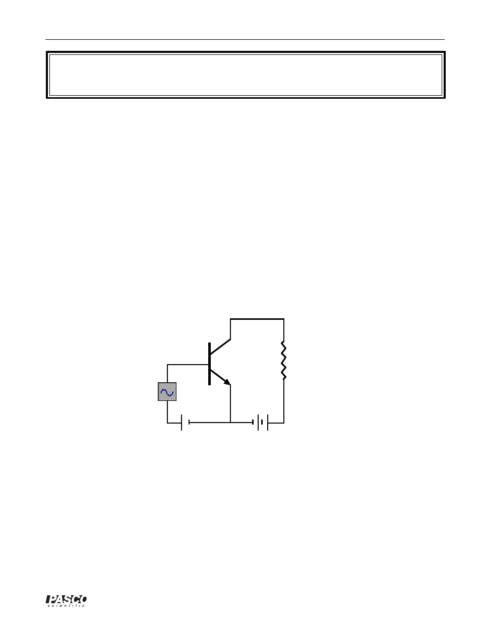
Base
Collector
Emitter
+
RL
npn Common-emitter amplifier
+
If the input voltage is small enough so that it is much smaller than the forward bias on the emitter
connection, the input current will encounter small impedance. The input voltage will not need to
be large in order to produce sizeable currents.
Additionally, since the output voltage across the load resistor R
L
is the product of the output
current (collector current) and the value of R
L
, the output voltage can also be made large. As a
result, the output voltage can be much larger than the input voltage.
The common-emitter amplifier derives its name from the fact that the base wire of the transistor
and the collector wire of the transistor meet at the emitter wire; they have the emitter wire in
common.