2 output signal allocations, Mecha – Yaskawa Sigma-5 User Manual: Design and Maintenance - Linear Motors MECHATROLINK-III Communications Reference User Manual
Page 70
3 Wiring and Connection
3.3.2 Output Signal Allocations
3-22
3.3.2 Output Signal Allocations
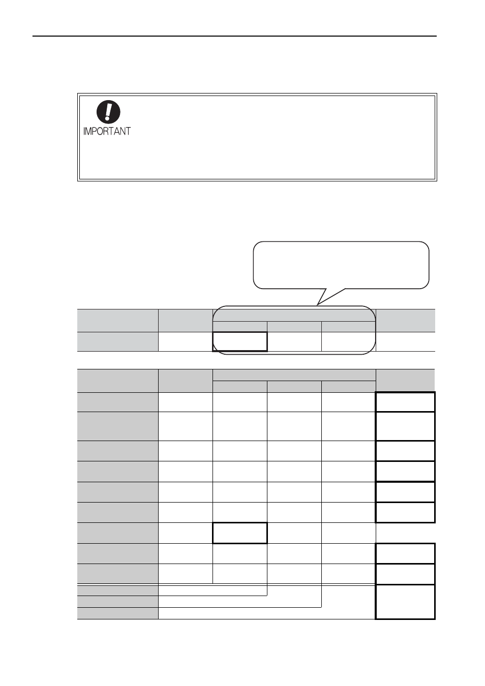
Output signals are allocated as shown in the following table.
Refer to the Interpreting the Output Signal Allocation Tables and change the allocations accordingly.
• The signals not detected are considered as "Invalid." For example, Positioning Com-
pletion (/COIN) signal in speed control is "Invalid."
• Inverting the polarity of the brake signal (/BK), i.e. positive logic, will prevent the hold-
ing brake from working in case of its signal line disconnection.
If this setting is absolutely necessary, check the operation and confirm that there are
no safety problems.
• When two or more signals are allocated to the same output circuit, a signal is output
with OR logic circuit.
Output Signal Names
and Parameters
Output Signal
CN1 Pin Numbers
Invalid
(not use)
1/ (2)
23/ (24)
25/ (26)
Positioning Completion
Pn50E.0
/COIN
1
2
3
0
Speed Coincidence
Detection
Pn50E.1
/V-CMP
1
2
3
0
Movement Detection
Pn50E.2
/TGON
1
2
3
0
Servo Ready
Pn50E.3
/S-RDY
1
2
3
0
Force Limit Detection
Pn50F.0
/CLT
1
2
3
0
Speed Limit Detection
Pn50F.1
/VLT
1
2
3
0
Brake
Pn50F.2
/BK
1
2
3
0
Warning
Pn50F.3
/WARN
1
2
3
0
Near
Pn510.0
/NEAR
1
2
3
0
Pn512.0=1
Polarity inversion of CN1-1(2)
0
(Not invert at
factory setting)
Pn512.1=1
Polarity inversion of CN1-23(24)
Pn512.2=1
Polarity inversion of CN1-25(26)
Output Signal
CN1 Pin Numbers
Invalid
㧔not use㧕
1/ (2)
23/ (24)
25/ (26)
Brake
Pn50F.2
/BK
1
2
3
0
The parameter set values to be used are shown.
Signals are allocated to CN1 pins according to the
selected set values.
Values in cells in bold lines are the factory settings.
Output Signal Names
and Parameters
MECHA