Simulating altera ip cores in other eda tools – Altera LVDS SERDES Transmitter / Receiver User Manual
Page 65
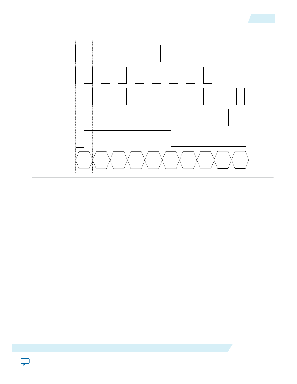
Figure 15: Phase Relationship for External PLL Interface Signals
D1
D2
D3
D4
D5
D6
D7
D8
D9
D10
inclk0
VCO clk
(internal PLL clk)
c0 (-180°
phase shift)
c1 (288°
phase shift)
c2 (-18°
phase shift)
Serial data
Related Information
•
•
Receiver Skew Margin and Transmitter Channel-to-Channel Skew
on page 54
External PLL Compensation Mode for ALTLVDS IP Core in External PLL Mode
If you instantiate the ALTLVDS IP core in external PLL mode, Altera recommends that you set up the
data rate and clocking with the PLL IP core.
Note: For Stratix IV, Arria II, and Cyclone IV devices, use the ALTPLL IP core. For Stratix V, Arria V,
and Cyclone V devices use the Altera PLL IP core.
• For Arria V, Arria V GZ, and Stratix V devices with ALTLVDS_RX configured in non-DPA mode, the
external PLL must be in LVDS compensation mode.
• For Cyclone V devices, LVDS interfaces placed on the all edges must be in LVDS compensation mode.
For more information about PLL compensation modes, refer to the PLL chapter of the relevant device
handbook.
Simulating Altera IP Cores in other EDA Tools
The Quartus II software supports RTL and gate-level design simulation of Altera IP cores in supported
EDA simulators. Simulation involves setting up your simulator working environment, compiling
simulation model libraries, and running your simulation.
UG-MF9504
2014.12.15
External PLL Compensation Mode for ALTLVDS IP Core in External PLL Mode
65
LVDS SERDES Transmitter/Receiver IP Cores User Guide
Altera Corporation