Latency, Pma latency, Pcs latency – Achronix Speedster22i SerDes User Manual
Page 42: Design flow: creating a serdes design, Design flow: creating a serdes, Design
Latency
This section presents the worst case latency for PMA and PCS blocks.
PMA Latency
The following equation calculates the worst-case latency for the Tx-datapth assuming the
case of first word in and last bit out:
𝑇𝑥
𝑤𝑜𝑟𝑠𝑡
= 𝐴𝑛𝑎𝑙𝑜𝑔_𝑙𝑎𝑡𝑒𝑛𝑐𝑦 + 2.5 ∗ 𝑑𝑎𝑡𝑎𝑏𝑢𝑠_𝑤𝑖𝑑𝑡ℎ ∗ 𝑈𝐼 + (𝑑𝑎𝑡𝑎𝑏𝑢𝑠_𝑤𝑖𝑑𝑡ℎ − 1) ∗ 𝑈𝐼 + 500𝑝𝑠,
where analog latency is explained below and 500 ps accounts for internal analog delay and
digital clock newtowrk latency.
The worst-case latency for the Rx-datapath can be calculated by the following equation
considering the case of first bit in and first word out:
𝑅𝑥
𝑤𝑜𝑟𝑠𝑡
= 5.5 𝑈𝐼 + 2.5 ∗ 𝑑𝑎𝑡𝑎𝑏𝑢𝑠_𝑤𝑖𝑑𝑡ℎ ∗ 𝑈𝐼 + (𝑑𝑎𝑡𝑎𝑏𝑢𝑠_𝑤𝑖𝑑𝑡ℎ − 1) ∗ 𝑈𝐼 + 500𝑝𝑠 ,
where 500 ps accounts for internal analog delay and digital clock newtowrk latency.
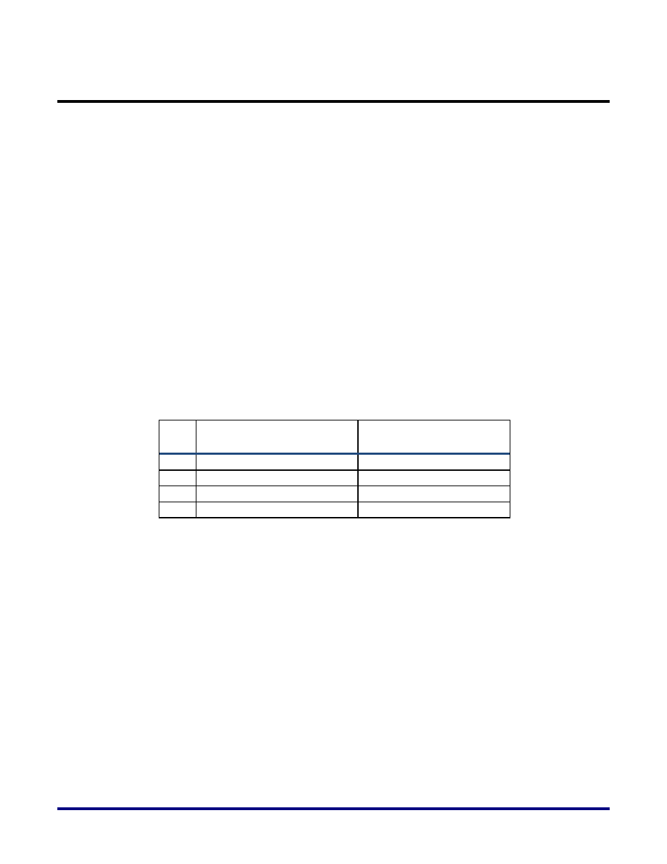
The analog latency is a function of the databus-width as well and can be estimated using
“Table 8: Analog latency as a function of databus width” below.
Table 8: Analog latency as a function of databus width
#
Databus Width
Analog Latency
1.
8-bit
28 UI
2.
10-bit
33 UI
3.
16-bit
36 UI
4.
20-bit
43 UI
As an example, for 20-bit databus width, the worst case latency for Tx and Rx datapath can
be estimated as follows:
𝑇𝑥
𝑤𝑜𝑟𝑠𝑡
= 43𝑈𝐼 + 50𝑈𝐼 + 19𝑈𝐼 + 500𝑝𝑠 = 112𝑈𝐼 + 500𝑝𝑠, and
𝑅𝑥
𝑤𝑜𝑟𝑠𝑡
= 5.5𝑈𝐼 + 50𝑈𝐼 + 19𝑈𝐼 + 500𝑝𝑠 = 73.5𝑈𝐼 + 500𝑝𝑠
Worst case values are presented in “Figure 20 Worst-case latency across PMA and PCS (in
PCS Latency
There are two modes of using PCS in Achronix SerDes:
1. PCS Enabled: All or selected PCS blocks can be enabled. Each block will introduce it’s
own latency in datapath. Even when selected blocks are disabled in this mode, data
(transmit and receive) will travel through the PCS components while bypassing them, as
shown in “Figure 6: - PCS Transmitter Block Overview”.
2. PCS Disabled: In this case, all PCS blocks are disabled. This mode introduces a latency of
2 clock-cycles.
42
UG028, July 1, 2014