Reference clock, Jitter specification, Table 29: reference clock electrical speficiations – Achronix Speedster22i SerDes User Manual
Page 112: Table 30: reference clock jitter specification
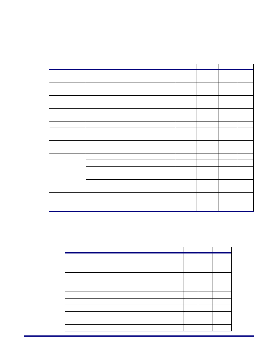
Reference Clock
The electrical specifications for the reference clock are summarized in the following tables
Table 29: Reference Clock Electrical Speficiations
Parameter
Description
Min
Typical
Max
Unit
F
REF
Reference clock operating frequency
range
50
250
MHz
T
REF
Reference clock operating frequency
range
4
20
ns
T
REF-DUTY
Duty Cycle
40
50
60
%
T
REF-RISE/FALL
Rise and falling edge rate
0.2
T
REF
T
REF-SINGLEEND-
SKEW
Skew between REFCLKP and REFCLKM
10
ps
T
REF-PPM-ERROR
Reference Clock Frequency Error
-5350
+350
ppm
Z
REF-SINGLEEND-DC
Reference Clock Input Impedance –
Terminated Mode
40
50
60
Ω
Z
REF-DIFF-DC
Reference Clock Input Impedance – High
Impedance Mode
>200k
Ω
V
REF-DIFF
Input Differential Voltage - PCIe
0.15
V
Input Differential Voltage - LVDS
0.25
0.4
V
Input Differential Voltage - LVPECL
0.525
0.95
V
V
REF-CM
Input Common Mode Voltage - PCIe
0.25
0.55
V
Input Common Mode Voltage - LVDS
1
1.4
V
Input Common Mode Voltage - LVPECL
1.84
2.1
V
T
REF-RMS-MAX
Total Integrated RMS Phase Noise for the
band of frequency ranging from 12kHz to
20MHz
0.7
ps
RMS
Jitter Specification
Table 30: Reference Clock Jitter Specification
Reference Clock Parameter
Typ
Max
Unit
Suggested RMS phase jitter at 333.3 MHz (12KHz to 20
MHz)
0.8
400 ps rms
Suggested cycle to cycle jitter at 333.3 MHz
51
ps p-p
SATA/SAS: cycle to cycle jitter
112
ps p-
p
SATA/SAS: deterministic jitter
40
ps p-p
FC: cycle-to-cycle jitter RMS
6
ps p-p
FC: deterministic jitter
5
ps p-p
PCI-Express Gen1: cycle to cycle jitter
150 ps p-p
PCI-Express Gen2: 10KHz – 1.5 MHz bandwidth
7.5
ps rms
PCI-Express Gen2: 1.5MHz – 2.5GHz bandwidth
4.0
ps rms
XFI: RMS random jitter (up to 100MHz)
10
ps rms
112
UG028, July 1, 2014