Clocking, Figure 17: serdes rx and tx clocks – Achronix Speedster22i SerDes User Manual
Page 36
Clocking
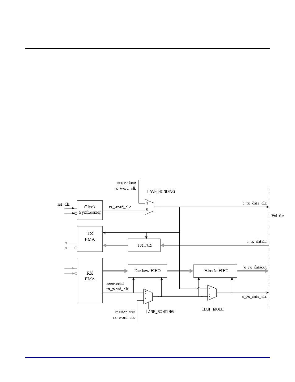
“Figure 17: SerDes RX and TX clocks” gives an overview of the clocks inside the SerDes. The
PMA of a SerDes lane generates two clocks, a TX word clock synthesized from the reference
clock, and an RX word clock recovered from the incoming serial data stream. The frequency
of these clocks is the data rate divided by the word width. For instance, a 10Gbps data rate
with 20 bit data width results in a 500MHz clock. Since the TX and RX clocks are generated
separately, they must be designated as unrelated in the timing constraints. In the most basic
mode, these TX and RX clocks are used to clock the data in their respective directions, and
are brought into the FPGA fabric for use by the user design.
Because each SerDes lane has its own PMA to generate a TX clock and an RX clock, the clocks
of different lanes are unrelated to each other, and consequently there is no synchronization
between the data of different lanes. Some protocols distribute data over a group of SerDes
lanes to increase bandwidth; typically, the lanes in such a group must then be synchronized
to give the appearance of a single high-bandwidth data stream. To synchronize multiple
SerDes lanes, Lane Bonding is used. As the Figure illustrates, when Lane Bonding is enabled,
a single lane is designated as master, and its TX and RX clocks are used to clock all the lanes
in the group. The deskew FIFO is used to convert data from the recovered clock domain to
the master RX domain; see Section “Deskew FIFO” for more details.
Figure 17: SerDes RX and TX clocks
36
UG028, July 1, 2014