Table 4, An269 – Cirrus Logic AN269 User Manual
Page 25
AN269
AN269REV1
25
A timing diagram for this type of display is shown in
. Signal and timing names are those of the
corresponding EP93xx pins. A description of the timing requirements is given in
In this type of display, the total number of SPCLKs per horizontal line is equal to the horizontal resolution.
Also, the total number of SPCLKs per full video frame is the horizontal resolution times the vertical resolu-
tion. Unlike an HSYNC/VSYNC-style display, there are no “extra” HSYNC or SPCLK pulses in the frame.
This will be accomplished by using a gated SPCLK, controlled by the HClkStrtStop register.
Note that in this timing, the VCSYNC signal actually comes after the HSYNC signal. To accomplish this, the
horizontal line counter is aligned such that line transitions occur at the VCSYNC transitions. This will be il-
lustrated in greater detail when the horizontal and vertical timings are determined.
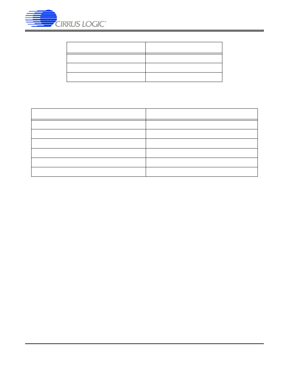
Display Pin
EP93xx Pin
CP
SPCLK
FRM
VCSYNC
LOAD
HSYNC
Table 4. Frame Type 1 Pin Mapping
Timing Parameter
Description
tHSYNCH
HSYNC High pulse duration
tHSYNCSPCLK
Time from HSYNC Low to first SPCLK on this line
tSPCLKHSYNC
Time from last SPCLK to HSYNC High on next line
tHVCSYNC
Time from HSYNC Low to VCSYNC High
tVCHSYNC
Time from VCSYNC High to HSYNC Falling Edge
tSPCLKHSYNC
Time from the last SPCLK to HSYNC Rising Edge
Table 5. Frame Type 1 Relevant Timing Parameters