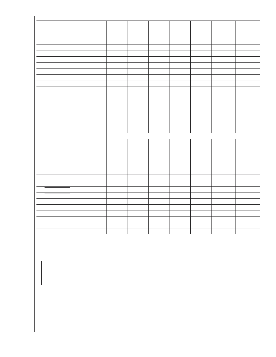
Note 9), Note 4), Note 5) – Rainbow Electronics LM93 User Manual
Page 90: Note, Note 10), Note 8), Note 12), Note 13), Note 14), Lm93
Symbol
Pin #
D1
D2
D4
D5
D6
SNP
R1
AD_IN1
23
U
U
U
U
U
AD_IN2
24
U
U
U
U
U
AD_IN3
25
U
U
U
U
U
AD_IN4
26
U
U
U
U
U
AD_IN5
27
U
U
U
U
U
AD_IN6
28
U
U
U
U
U
AD_IN7
29
U
U
U
U
U
AD_IN8
30
U
U
U
U
U
AD_IN9
31
U
U
U
U
U
AD_IN10
32
U
U
U
U
U
AD_IN11
33
U
U
U
U
U
AD_IN12
34
U
U
U
U
U
AD_IN13
35
U
U
U
U
U
AD_IN14
36
U
U
U
U
U
AD_IN15
37
U
U
U
U
U
ADDR_SEL
38
U
U
AD_IN16/V
DD
(V+)
39
U
U
U
U
GND
40
Internally shorted to AGND.
PWM1
41
U
U
U
50
Ω
PWM2
42
U
U
U
50
Ω
P1_VID0
43
U
U
P1_VID1
44
U
U
P1_VID2
45
U
U
P1_VID3
46
U
U
P1_VID4
47
U
U
P1_VID5
48
U
U
P1_PROCHOT
49
U
U
U
50
Ω
P2_PROCHOT
50
U
U
U
50
Ω
P2_VID0
51
U
U
P2_VID1
52
U
U
P2_VID2
53
U
U
P2_VID3
54
U
U
P2_VID4
55
U
U
P2_VID5
56
U
U
Note 4: Human body model, 100 pF discharged through a 1.5 k
Ω resistor. Machine model, 200 pF discharged directly into each pin.
Note 5: Reflow temperature profiles are different for lead-free and non lead-free packages.
Note 6: The maximum power dissipation must be de-rated at elevated temperatures and is dictated by T
JMAX
,
θ
JA
and the ambient temperature, T
A
. The maximum
allowable power dissipation at any temperature is PD = (T
JMAX
− T
A
) /
θ
JA
. The
θ
JA
for the LM93 when mounted to 1 oz. copper foil PCB the
θ
JA
with different air
flow is listed in the following table.
Air Flow
Junction to Ambient Thermal Resistance,
θ
JA
0 m/s
79 ˚C/W
1.14 m/s (225 LFPM)
62 ˚C/W
2.54 m/s (500 LFPM)
52 ˚C/W
Note 7: See the URL "http://www.national.com/packaging/" for other recommendations and methods of soldering surface mount devices.
Note 8: When measuring an MMBT3904 transistor, 4 ˚C should be subracted from all temperature readings.
Note 9: Typical parameters are at T
J
= T
A
= 25 ˚C and represent most likely parametric norm.
Note 10: Limits are guaranteed to National’s AOQL (Average Outgoing Quality Level).
Note 11: TUE (Total Unadjusted Error) includes Offset, Gain and Linearity errors of the ADC.
Note 12: Total Monitoring Cycle Time includes all temperature and voltage conversions.
Note 13: Leakage current approximately doubles every 20 ˚C.
Note 14: A total digital I/O current of 40mA can cause 6mV of offset in Vref.
LM93
www.national.com
90