Voltage vs register reading, 0 functional description – Rainbow Electronics LM93 User Manual
Page 13

12.0 Functional Description
(Continued)
provide a nominal
3
⁄
4
full scale reading, while the −12V
should be scaled to provide a nominal
1
⁄
4
scale reading. The
thevenin resistance at the pin should be kept between 1 k
Ω
and 7 k
Ω.
The −12V monitoring is particularly challenging. It is required
that an external offset voltage and external resistors be used
to bring the −12V rail into the positive input voltage region of
the A/D input. It is suggested that the supply rail for the LM93
device be used as the offset voltage. This voltage is usually
derived from the P/S 5V stand-by voltage rail via a
±
1%
accurate linear regulator. In this fashion we can always
assume that the offset voltage is present when the −12V rail
is present as the system cannot be turned on without the
3.3V stand-by voltage being present.
Voltage vs Register Reading
Pin
Normal
Use
Nominal
Voltage
Register
Reading
at
Nominal
Voltage
Maximum
Voltage
Register
Reading at
Maximum
Voltage
Minimum
Voltage
Register
Reading at
Minimum
Voltage
Absolute
Maxmum Range
AD_IN1
+12V1
0.927V
C0h
1.236V
FFh
0V
00h
−0.3V to (V
DD
+ 0.05V)
AD_IN2
+12V2
0.927V
C0h
1.236V
FFh
0V
00h
−0.3V to (V
DD
+ 0.05V)
AD_IN3
+12V3
0.927V
C0h
1.236V
FFh
0V
00h
−0.3V to (V
DD
+ 0.05V)
AD_IN4
FSB_Vtt
1.20V
C0h
1.60V
FFh
0V
00h
−0.3V to +6.0V
AD_IN5
3GIO
1.5V
C0h
2V
FFh
0V
00h
−0.3V to +6.0V
AD_IN6
ICH_Core
1.5V
C0h
2V
FFh
0V
00h
−0.3V to +6.0V
AD_IN7
Vccp1
1.20V
C0h
1.60V
FFh
0V
00h
−0.3V to +6.0V
AD_IN8
Vccp2
1.20V
C0h
1.60V
FFh
0V
00h
−0.3V to +6.0V
AD_IN9
+3.3V
3.30V
C0h
4.40V
FFh
0V
00h
−0.3V to +6.0V
AD_IN10
+5V
5.0V
C0h
6.667V
FAh
0V
00h
−0.3V to +6.5V
AD_IN11
SCSI_Core
2.5V
C0h
3.333V
FFh
0V
00h
−0.3V to +6.0V
AD_IN12
Mem_Core
1.969V
C0h
2.625V
FFh
0V
00h
−0.3V to +6.0V
AD_IN13
Mem_Vtt
0.984V
C0h
1.312V
FFh
0V
00h
−0.3V to +6.0V
AD_IN14
Gbit_Core
0.984V
C0h
1.312V
FFh
0V
00h
−0.3V to +6.0V
AD_IN15
−12V
0.309V
40h
1.236V
FFh
0V
00h
−0.3V to (V
DD
+ 0.05V)
AD_IN16
+3.3V S/B
3.3V
C0h
3.6V
D1h
3.0V
AEh
−0.3V to +6.0V
Application Note: The nominal voltages listed in this table are only typical values. Voltage rails with different nominal voltages can be monitored, but the register
reading at the nominal value is no longer C0h. For example, a Mem_Core rail at 2.5V nominal could be monitored with AD_IN12, or a Mem_Vtt rail at 1.2V could
be monitored with AD_IN13.
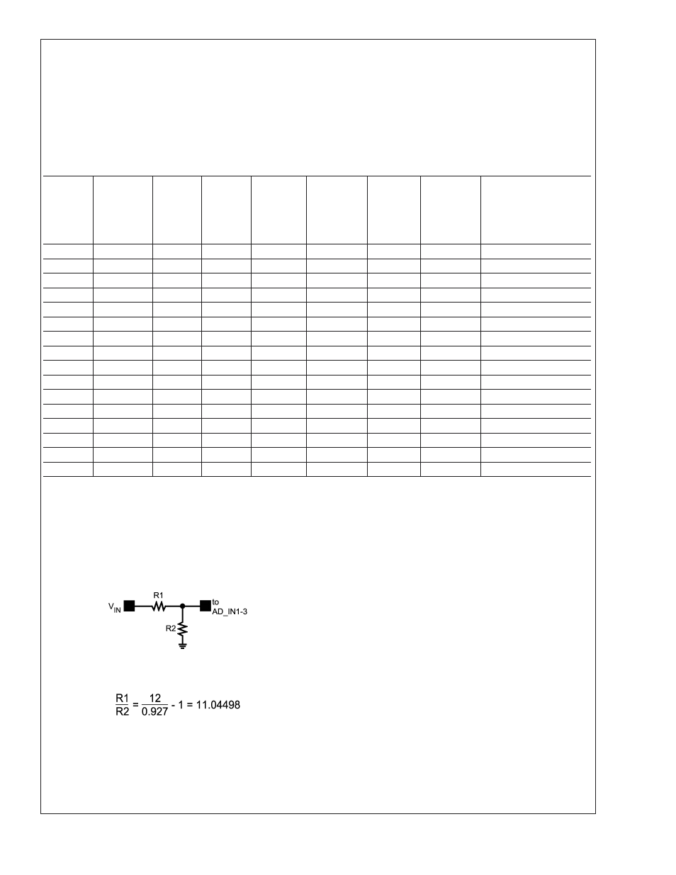
12.5 RECOMMENDED EXTERNAL SCALING RESISTORS FOR +12V POWER RAILS
The +12V inputs require external scaling resistors. The re-
sistors need to scale 12V down to 0.927V.
Required External Scaling
Resistors for +12V Power Input
20068208
To calculate the required ratio of R1 to R2 use this equation:
It is recommended that the equivalent thevenin resistance of
the divider be between 1k and 7k to minimize errors caused
by leakage currents at extreme temperatures. The best val-
ues for the resistors are: R1=13.7 k
Ω and R2=1.15 kΩ. This
yields a ratio of 11.94498, which has a +0.27% deviation
from the theoretical. It is also recommended that the resis-
tors have
±
1% tolerance or better.
Each LSB in the voltage value registers has a weight of 12V
/ 192 = 62.5 mV. To calculate the actual voltage of the +12V
power input, use the following equation:
V
IN
= (8-bit value register code) x (62.5 mV)
12.6 RECOMMENDED EXTERNAL SCALING CIRCUIT
FOR −12V POWER INPUT
The −12V input requires external resistors to level shift the
nominal input voltage of −12V to +0.309V.
LM93
www.national.com
13
