Ds1876 sfp controller with dual ldd interface – Rainbow Electronics DS1876 User Manual
Page 62
62 _____________________________________________________________________________________
DS1876
SFP Controller with Dual LDD Interface
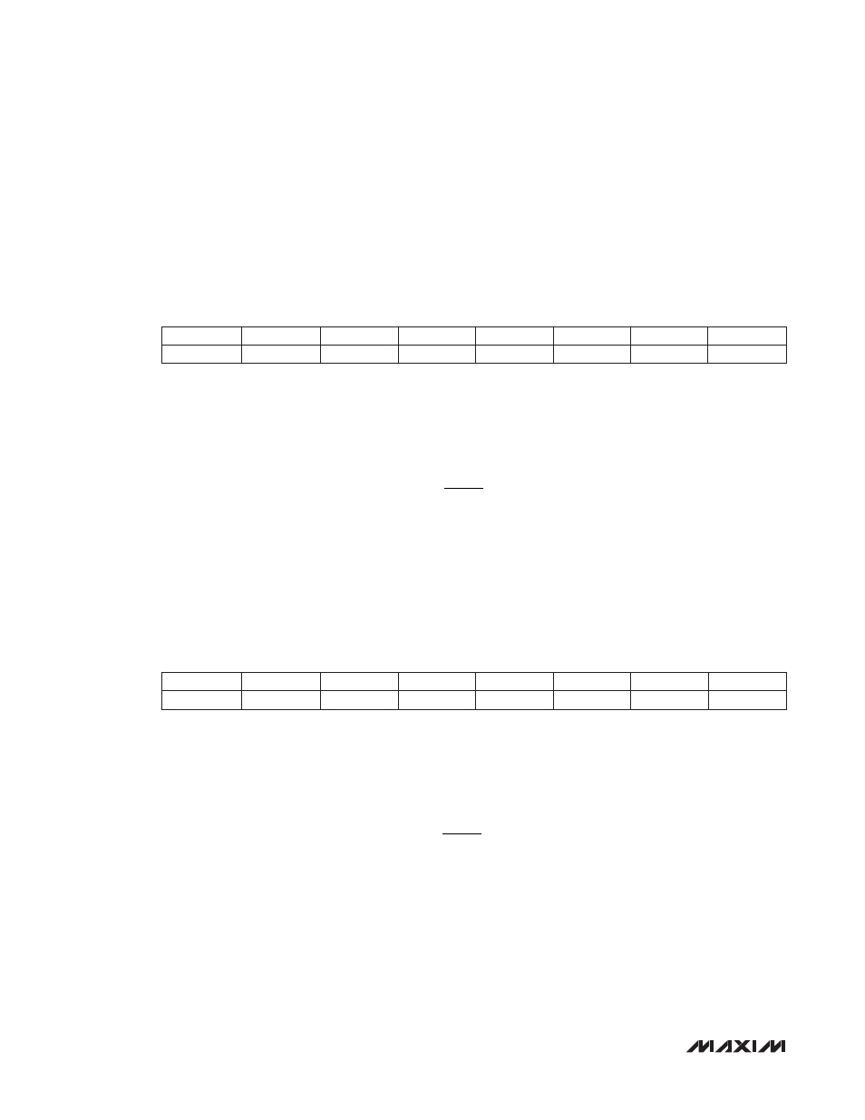
Table 02h, Register CAh–CBh: APC2 DAC
Table 02h, Register CCh–CDh: MOD1 DAC
FACTORY DEFAULT
0000h
READ ACCESS
PW2 or (PW1 and RWTBL2) or (PW1 and RTBL2)
WRITE ACCESS
(PW2 and APC2EN = 0) or (PW1 and RWTBL2 and APC2EN = 0)
A2h AND B2h MEMORY
Common A2h and B2h memory location
MEMORY TYPE
Volatile
CAh
0
0
0
0
0
0
2
9
2
8
CBh
2
7
2
6
2
5
2
4
2
3
2
2
2
1
2
0
BIT 7
BIT 0
The digital value used for APC2 DAC. It is the result of LUT6 plus APC2 OFFSET times 4 recalled from Table
06h (Registers F8h–FFh) at the adjusted memory address found in TINDEX. This register is updated at the end
of the temperature conversion.
APC2 DAC = LUT6 + APC2 OFFSET x 4
REFIN
APC2
V
V
APC2 DAC
1024
=
×
FACTORY DEFAULT
0000h
READ ACCESS
PW2 or (PW1 and RWTBL2) or (PW1 and RTBL2)
WRITE ACCESS
(PW2 and MOD1EN = 0) or (PW1 and RWTBL2 and MOD1EN = 0)
A2h AND B2h MEMORY
Common A2h and B2h memory location
MEMORY TYPE
Volatile
CCh
0
0
0
0
0
0
2
9
2
8
CDh
2
7
2
6
2
5
2
4
2
3
2
2
2
1
2
0
BIT 7
BIT 0
The digital value used for MOD1 DAC. It is the result of LUT4 plus MOD1 OFFSET times 4 recalled from Table
04h (Registers F8h–FFh) at the adjusted memory address found in TINDEX. This register is updated at the end
of the temperature conversion.
MOD1 DAC = LUT4 + MOD1 OFFSET x 4
REFIN
MOD1
V
V
MOD1 DAC
1024
=
Ч