Register descriptions, Memory map access codes, Memory addresses a0h, a2h, and b2h – Rainbow Electronics DS1876 User Manual
Page 24: Ds1876 sfp controller with dual ldd interface
24 _____________________________________________________________________________________
DS1876
SFP Controller with Dual LDD Interface
Register Descriptions
The register maps show each byte/word (2 bytes) in
terms of its row in the memory. The first byte in the row
is located in memory at the row address (hexadecimal)
in the leftmost column. Each subsequent byte on the row
is one/two memory locations beyond the previous byte/
word’s address. A total of 8 bytes are present on each
row. For more information about each of these bytes, see
the corresponding register description.
Memory Map Access Codes
The following section provides the DS1876 register defi-
nitions. Each register or row of registers has an access
descriptor that determines the password level required
to read or write the memory. Level 2 password is
intended for the module manufacture access only. Level
1 password allows another level of protection for items
the end consumer wishes to protect. Many registers are
always readable, but require password access to write.
There are a few registers that cannot be read without
password access. The following access codes describe
each mode used by the DS1876 with factory settings for
the PW_ENA and PW_ENB (Table 02h, Registers C0h–
C1h) registers.
Memory Addresses A0h, A2h, and B2h
There are three separate I
2
C addresses in the DS1876:
A0h, A2h, and B2h. A2h and B2h are used to configure
and monitor two transmitters. Transmitter 1 is accessed
using A2h. Transmitter 2 is accessed using B2h. Many
of the registers in A2h and B2h are shared registers.
These registers can be read and written from both A2h
and B2h.
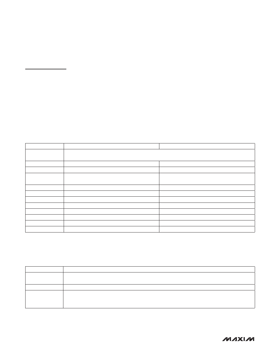
ACCESS CODE
READ ACCESS
WRITE ACCESS
<0/_>
At least 1 byte/bit in the row/byte is different than the rest of the row/byte, so look at each byte/bit
separately for permissions.
<1/_>
Read all
Write PW2
<2/_>
Read all
Write not applicable
<3/_>
Read all
Write all, but the DS1876 hardware also writes to
these bytes/bits
<4/_>
Read PW2
Write PW2 + mode_bit
<5/_>
Read all
Write all
<6/_>
Read not applicable
Write all
<7/_>
Read PW1
Write PW1
<8/_>
Read PW2
Write PW2
<9/_>
Read not applicable
Write PW2
<10/_>
Read PW2
Write not applicable
<11/_>
Read all
Write PW1
MEMORY CODE
A2h AND B2h REGISTERS
A common memory location is used for A2h and B2h device addresses. Reading or writing to these
locations is identical, regardless of using A2h or B2h addresses.
Different memory locations are used for A2h and B2h device addresses.
Mixture of common and different memory locations for A2h and B2h device addresses. See the individual
bytes within the row for clarification. If “M” is used on an individual byte, see the expanded bit descriptions
to determine which bits are common vs. different.