Ds1876 sfp controller with dual ldd interface – Rainbow Electronics DS1876 User Manual
Page 57
______________________________________________________________________________________ 57
DS1876
SFP Controller with Dual LDD Interface
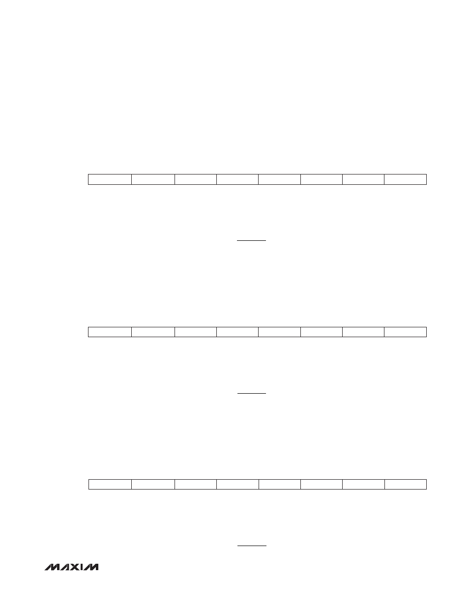
Table 02h, Register BDh: HBIAS1 DAC
Table 02h, Register BEh: HTXP1 DAC
Table 02h, Register BFh: LTXP1 DAC
FACTORY DEFAULT
00h
READ ACCESS
PW2 or (PW1 and RWTBL2) or (PW1 and RTBL2)
WRITE ACCESS
(PW2 and QT1EN = 0) or (PW1 and RWTBL2 and QT1EN = 0)
A2h AND B2h MEMORY
Common A2h and B2h memory location
MEMORY TYPE
Volatile
BDh
2
7
2
6
2
5
2
4
2
3
2
2
2
1
2
0
BIT 7
BIT 0
The digital value used for the HBIAS1 reference and recalled from Table 06h (Registers E0h–E7h) (transmitter 1) at
the adjusted memory address found in TINDEX. This register is updated at the end of the temperature conversion.
Comparisons greater than V
HBIAS1
compared against V
BMON1
create an HBAL alarm.
HBIAS1
Full Scale
V
HBIAS1 DAC
256
=
×
FACTORY DEFAULT
00h
READ ACCESS
PW2 or (PW1 and RWTBL2) or (PW1 and RTBL2)
WRITE ACCESS
(PW2 and QT1EN = 0) or (PW1 and RWTBL2 and QT1EN = 0)
A2h AND B2h MEMORY
Common A2h and B2h memory location
MEMORY TYPE
Volatile
BEh
2
7
2
6
2
5
2
4
2
3
2
2
2
1
2
0
BIT 7
BIT 0
The digital value used for the HTXP1 reference and recalled from Table 06h (Registers E8h–EFh) (transmitter 1) at
the adjusted memory address found in TINDEX. This register is updated at the end of the temperature conversion.
Comparisons great than V
HTXP1
compared against V
PMON1
create a TXP HI alarm.
HTXP1
Full Scale
V
HTXP1 DAC
256
=
×
FACTORY DEFAULT
00h
READ ACCESS
PW2 or (PW1 and RWTBL2) or (PW1 and RTBL2)
WRITE ACCESS
(PW2 and QT1EN = 0) or (PW1 and RWTBL2 and QT1EN = 0)
A2h AND B2h MEMORY
Common A2h and B2h memory location
MEMORY TYPE
Volatile
BFh
2
7
2
6
2
5
2
4
2
3
2
2
2
1
2
0
BIT 7
BIT 0
The digital value used for the LTXP1 reference and recalled from Table 06h (Registers F0h–F7h) (transmitter 1) at
the adjusted memory address found in TINDEX. This register is updated at the end of the temperature conversion.
Comparisons less than V
LTXP1
compared against V
PMON1
create a TXP LO alarm.
LTXP1
Full Scale
V
LTXP1 DAC
256
=
Ч