Ds1876 sfp controller with dual ldd interface – Rainbow Electronics DS1876 User Manual
Page 34
34 _____________________________________________________________________________________
DS1876
SFP Controller with Dual LDD Interface
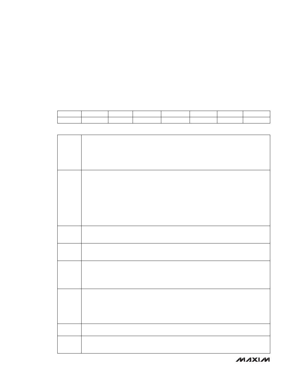
Lower Memory, Register 6Eh: STATUS
POWER-ON VALUE
X0XX 0XXXb
READ ACCESS
All
WRITE ACCESS
See below
A2h AND B2h MEMORY
Mixture of common memory locations and different memory locations (see below)
MEMORY TYPE
Volatile
Write Access
N/A
All
N/A
All
All
N/A
N/A
N/A
6Eh
TXDS
TXDC
IN1S
RSELS
RSELC
TXFS
RAM
RDYB
BIT 7
BIT 0
BIT 7
TXDS1 [A2h]: TXD1 status bit. Reflects the logic state of the TXD1 pin (read-only).
0 = TXD1 pin is logic-low.
1 = TXD1 pin is logic-high.
TXDS2 [B2h]: TXD2 status bit. Reflects the logic state of the TXD2 pin (read-only).
0 = TXD2 pin is logic-low.
1 = TXD2 pin is logic-high.
BIT 6
TXDC1 [A2h]: TXD1 software control bit. This bit allows for software control that is identical to the
TXD1 pin. See the DACs as a Function of Transmit Disable (TXD1, TXD2) section for further infor-
mation. Its value is wire-ORed with the logic value of the TXD1 pin (writable by all users).
0 = (default)
1 = Forces the device into a TXD1 state regardless of the value of the TXD1 pin.
TXDC2 [B2h]: TXD2 software control bit. This bit allows for software control that is identical to the
TXD2 pin. See the DACs as a Function of Transmit Disable (TXD1, TXD2) section for further infor-
mation. Its value is wire-ORed with the logic value of the TXD2 pin (writable by all users).
0 = (default)
1 = Forces the device into a TXD2 state regardless of the value of the TXD2 pin.
BIT 5
IN1S [A2h or B2h]: IN1 status bit. Reflects the logic state of the IN1 pin (read-only).
0 = IN1 pin is logic-low.
1 = IN1 pin is logic-high.
BIT 4
RSELS [A2h or B2h]: RSEL status bit. Reflects the logic state of the RSEL pin (read-only).
0 = RSEL pin is logic-low.
1 = RSEL pin is logic-high.
BIT 3
RSELC [A2h or B2h]: RSEL software control bit. This bit allows for software control that is iden-
tical to the RSEL pin. Its value is wire-ORed with the logic value of the RSEL pin to create the
RSELOUT pin’s logic value (writable by all users).
0 = (default)
1 = Forces the device into a RSEL state regardless of the value of the RSEL pin.
BIT 2
TXFS1 [A2h]: Reflects state of the TXF1 pin (read-only).
0 = TXF1 pin is low.
1 = TXF1 pin is high.
TXFS2 [B2h]: Reflects the state of the TXF2 pin (read-only).
0 = TXF2 pin is low.
1 = TXF2 pin is high.
BIT 1
RAM1 [A2h]: Volatile memory location.
RAM2 [B2h]: Volatile memory location.
BIT 0
RDYB [A2h or B2h]: Ready bar.
0 = V
CC
is above POA.
1 = V
CC
is below POA and/or too low to communicate over the I
2
C bus.