Ds1876 sfp controller with dual ldd interface – Rainbow Electronics DS1876 User Manual
Page 47
______________________________________________________________________________________ 47
DS1876
SFP Controller with Dual LDD Interface
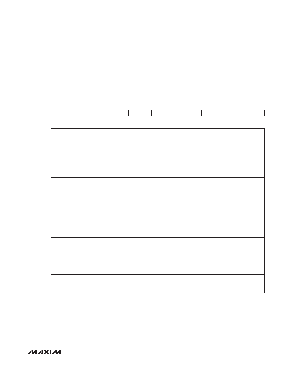
Table 02h, Register 88h: CNFGA
FACTORY DEFAULT
C0h
READ ACCESS
PW2 or (PW1 and RWTBL2) or (PW1 and RTBL2)
WRITE ACCESS
PW2 or (PW1 and RWTBL2)
A2h AND B2h MEMORY
Common A2h and B2h memory location
MEMORY TYPE
Nonvolatile (SEE)
88h
QTHEXT2
QTHEXT1
RESERVED
ASEL
MASK
INVRSOUT
INVTXFOUT2
INVTXFOUT1
BIT 7
BIT 0
BIT 7
QTHEXT2: QT high extension for transmitter 2.
0 = Disabled. TXP HI and HBIAS QT alarms of transmitter 2 immediately create FETG.
1 = (default) Enabled. TXP HI and HBIAS QT alarms of transmitter 2 do not create FETG until the
timeout of the TXD
EXT
time interval.
BIT 6
QTHEXT1: QT high extension for transmitter 1.
0 = Disabled. TXP HI and HBIAS QT alarms of transmitter 1 immediately create FETG.
1 = (default) Enabled. TXP HI and HBIAS QT alarms of transmitter 1 do not create FETG until the
timeout of the TXD
EXT
time interval.
BIT 5
RESERVED
BIT 4
ASEL: Address select.
0 = (default) Device address is A2h for transmitter 1 and B2h for transmitter 2.
1 = The DEVICE ADDRESS register (Table 02h, Register 8Bh) is used to determine the main device
address.
BIT 3
MASK:
0 = (default) Alarm-enable row exists at Table 01h, Registers F8h–FFh. Table 05h, Registers F8h–
FFh are empty.
1 = Alarm-enable row exists at Table 05h, Registers F8h–FFh. Table 01h, Registers F8h–FFh are
empty.
BIT 2
INVRSOUT: Allow for inversion of the RSELOUT pin (see Figure 10).
0 = (default) RSELOUT is not inverted.
1 = RSELOUT is inverted.
BIT 1
INVTXFOUT2: Allow for inversion of signal driven by the TXF2 input pin.
0 = (default) TXF2 signal is not inverted.
1 = TXF2 signal is inverted.
BIT 0
INVTXFOUT1: Allow for inversion of signal driven by the TXF1 input pin.
0 = (default) TXF1 signal is not inverted.
1 = TXF1 signal is inverted.