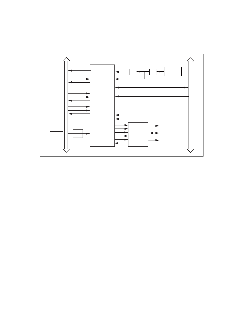
Figure 3-17. timing i/o circuitry block diagram – National Instruments AT-MIO-16X User Manual
Page 92

Chapter 3
Theory of Operation
AT-MIO-16X User Manual
3-26
© National Instruments Corporation
Figure 3-17. Timing I/O Circuitry Block Diagram
The Am9513A contains five independent 16-bit counter/timers, a 4-bit
frequency output channel, and five internally generated timebases. The
five counter/timers can be programmed to operate in several useful
timing modes. The programming and operation of the Am9513A are
presented in detail in Appendix C, AMD Am9513A Data Sheet.
The Am9513A clock input is one-tenth the BRDCLK frequency.
BRDCLK is selected through a register in the AT-MIO-16X register
set. The factory default for BRDCLK is 10 MHz, which generates a
1-MHz clock input to the Am9513A. The Am9513A uses this clock
input plus a BRDCLK divided-by-two input at Source 2 to generate
six internal timebases. These timebases can be used as clocks by the
counter/timers and by the frequency output channel. When BRDCLK
is 10 MHz, the six internal timebases normally used for AT-MIO-16X
timing functions are 5 MHz, 1 MHz, 100 kHz, 10 kHz, 1 kHz, and
100 Hz. The 16-bit counters in the Am9513A can be diagrammed as
shown in Figure 3-18.
GATE4
RTSI Bus
/
2
/
16
1 MHz
DATA<15..0>
Am9513A RD/WR
CONVERT
SCANCLK
CONFIGCLK
Data
Acquisition
Timing
SOURCE4
SOURCE3
OUT1
OUT2
OUT3
OUT4
OUT5
GATE3
Am9513A
Five-Channel
Counter/
Timer
GATE5
SOURCE5
OUT5
GATE2
OUT2
GATE1
SOURCE1
OUT1
FOUT
I/O Connector
EXTTRIG*
Flip
Flop
GATE4
PC I/O Channel
BRDCLK
(10 MHz)
ч
5
ч
2
SOURCE2
5 MHz
