Figure 5-10. rtsi switch control pattern, Figure 5-10. rtsi switch control pattern -40 – National Instruments AT-MIO-16X User Manual
Page 209

Chapter 5
Programming
AT-MIO-16X User Manual
5-40
© National Instruments Corporation
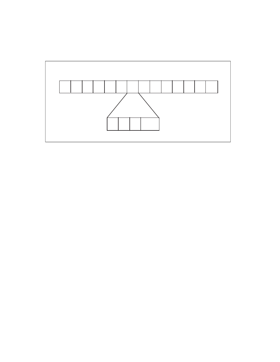
Figure 5-10. RTSI Switch Control Pattern
In Figure 5-10, the fields labeled A6 through A0 and B6 through B0 are
the 4-bit control fields for each RTSI switch pin of the same name. The
4-bit control field for pin A0 is shown in Figure 5-10.
The bits labeled S2 through S0 are the signal source selection bits for
the pin. One of seven source signals can be selected. Pins A6 through
A0 can select any of the pins B6 through B0 as signal sources. Pins B6
through B0 select any of the pins A6 through A0 as signal sources. For
example, the pattern 011 for S2 through S0 in the A0 control field
selects the signal connected to pin B3 as the signal source for pin A0.
The bit labeled OUTEN is the output enable bit for that pin. If the
OUTEN bit is set, the pin is driven by the selected source signal (the pin
acts as an output pin). If the OUTEN bit is cleared, the pin is not driven
regardless of the source signal selected; instead, the pin can be used as
an input pin.
If the preceding A0 control field contains the pattern 0111, the signal
connected to pin B3 (Trigger Line 3) appears at pin A0. On the
AT-MIO-16X board, this arrangement allows the EXTCONV* signal to
be driven by Trigger Line 3. Conversely, if the B4 control field contains
the pattern 1011, the signal connected to pin A5 appears at pin B4. This
arrangement allows Trigger Line 4 to be driven by the AT-MIO-16X
OUT1 signal. In this way, boards connected via the RTSI bus can send
signals to each other over the RTSI bus trigger lines.
A6
A5
A4
A3
A2
A1
A0
B6
B5
B4
B3
B2
B1
B0
A0 Control
S2
S1
S0 OUTEN
Bit Number
31
30
29
28
Bit Number
55
51
47
43
39
35
31
27
23
19
15
11
7
3
0
MSB
LSB
