Epson S1C63558 User Manual
Page 98
88
EPSON
S1C63558 TECHNICAL MANUAL
CHAPTER 4: PERIPHERAL CIRCUITS AND OPERATION (Serial Interface)
Data receive procedure
The control procedure and operation during receiving is as follows.
(1) Write "0" in the receive enable register
RXEN to set the receiving disable status
and to reset the respective PER, OER,
FER flags that indicate parity, overrun
and framing errors.
(2) Write "1" in the receive enable register
RXEN to set into the receiving enable
status.
(3) The shift clock will change to enable
from the point where the start bit
(LOW) has been input from the SIN
terminal and the receive data will be
synchronized to the rising edge follow-
ing the second clock, and will thus be
successively incorporated into the shift
register.
After data bits have been incorporated,
the stop bit is checked and, if it is not
HIGH, it becomes a framing error and the
error interrupt factor flag ISER is set to
"1". When interrupt has been enabled, an
error interrupt is generated at this point.
When receiving is completed, data in
the shift register is transferred to the
receive data buffer and the receiving
complete interrupt flag ISRC is set to
"1". When interrupt has been enabled, a
receiving complete interrupt is gener-
ated at this point. (When an overrun
error is generated, the interrupt factor
flag ISRC is not set to "1" and a receiv-
ing complete interrupt is not gener-
ated.)
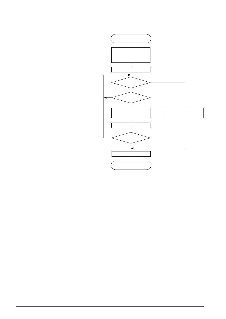
End
RXEN
←
1
No
Yes
Receiving interrupt ?
Yes
Receiving complete ?
Received data reading
from TRXD0–TRXD7
RXEN
←
0
RXTRG
←
1
No
Yes
Error generated ?
Error processing
Data receiving
RXEN
←
0
Resets error flags
PER, OER and FER
No
If "with parity check" has been selected, a parity check is executed when data is transferred into the
receive data buffer from the shift register and if a parity error is detected, the error interrupt factor
flag is set to "1". When the interrupt has been enabled, an error interrupt is generated at this point just
as in the framing error mentioned above.
(4) Read the received data from TRXD0–TRXD7 using receiving complete interrupt.
(5) Write "1" to the receive control bit RXTRG to inform that the receive data has been read out.
When the following data is received prior to writing "1" to RXTRG, it is recognized as an overrun
error and the error interrupt factor flag is set to "1". When the interrupt has been enabled, an error
interrupt is generated at this point just as in the framing error and parity error mentioned above.
(6) Repeat steps (3) to (5) for the number of bytes of receiving data, and then set the receive disable status
by writing "0" to the receive enable register RXEN, when the receiving is completed.
Fig. 4.11.7.3 Receiving procedure in asynchronous mode