7 i/o memory of sound generator – Epson S1C63558 User Manual
Page 115

S1C63558 TECHNICAL MANUAL
EPSON
105
CHAPTER 4: PERIPHERAL CIRCUITS AND OPERATION (Sound Generator)
4.12.7 I/O memory of sound generator
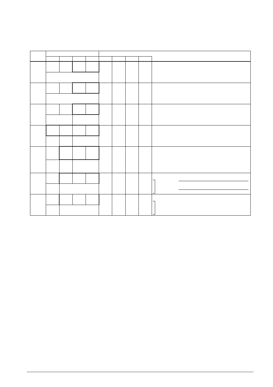
Table 4.12.7.1 shows the I/O addresses and the control bits for the sound generator.
Table 4.12.7.1 Control bits of sound generator
Address
Comment
D3
D2
Register
D1
D0
Name
Init
∗
1
1
0
FF30H
R03HIZ R02HIZ R01HIZ R00HIZ
R/W
R03HIZ
R02HIZ
R01HIZ
R00HIZ
0
0
0
0
Hi-Z
Hi-Z
Hi-Z
Hi-Z
Output
Output
Output
Output
R03 (FOUTE=0)/FOUT (FOUTE=1) Hi-z control
R02 (PTOUT=0)/TOUT (PTOUT=1) Hi-z control
R01 (BZOUT=0)/BZ (BZOUT=1) Hi-z control
R00 (XBZOUT=0)/XBZ (XBZOUT=1) Hi-z control
FF31H
R03
(FOUT)
R02
(TOUT)
R01
(BZ)
R00
(XBZ)
R/W
R03
R02
R01
R00
1
1
1
1
High
High
High
High
Low
Low
Low
Low
R03 output port data (FOUTE=0) Fix at "1" when FOUT is used.
R02 output port data (PTOUT=0) Fix at "1" when TOUT is used.
R01 output port data (BZOUT=0) Fix at "1" when BZ is used.
R00 output port data (XBZOUT=0) Fix at "1" when XBZ is used.
FF65H
0
0
BZOUT XBZOUT
R
R/W
0
∗
3
0
∗
3
BZOUT
XBZOUT
–
∗
2
–
∗
2
0
0
BZ
XBZ
DC
DC
Unused
Unused
R01 output selection (R01 should be fixed at "1".)
R00 output selection (R00 should be fixed at "1".)
FF6EH
0
BZFQ2
BZFQ1
BZFQ0
R
R/W
0
∗
3
BZFQ2
BZFQ1
BZFQ0
–
∗
2
0
0
0
FF6FH
0
BDTY2
BDTY1
BDTY0
R
R/W
0
∗
3
BDTY2
BDTY1
BDTY0
–
∗
2
0
0
0
FF6CH
ENRTM ENRST
ENON
BZE
R/W
W
R/W
ENRTM
ENRST
∗
3
ENON
BZE
0
Reset
0
0
1sec
Reset
On
Enable
0.5sec
Invalid
Off
Disable
Envelope releasing time selection
Envelope reset (writing)
Envelope On/Off
Buzzer output enable
FF6DH
0
BZSTP BZSHT SHTPW
R
W
R/W
0
∗
3
BZSTP
∗
3
BZSHT
SHTPW
–
∗
2
0
0
0
Stop
Trigger
Busy
125msec
Invalid
Invalid
Ready
31.25msec
Unused
1-shot buzzer stop (writing)
1-shot buzzer trigger (writing)
1-shot buzzer status (reading)
1-shot buzzer pulse width setting
0
4096.0
1
3276.8
2
2730.7
3
2340.6
[BZFQ2, 1, 0]
Frequency (Hz)
4
2048.0
5
1638.4
6
1365.3
7
1170.3
[BZFQ2, 1, 0]
Frequency (Hz)
Unused
Buzzer
frequency
selection
Unused
Buzzer signal duty ratio selection
(refer to main manual)
*1 Initial value at initial reset
*2 Not set in the circuit
*3 Constantly "0" when being read
R00HIZ, R01HIZ: R00, R01 port high impedance control register (FF30H•D0, D1)
Controls high impedance output of the output port.
When "1" is written: High impedance
When "0" is written: Data output
Reading: Valid
When using the BZ and XBZ outputs, fix the registers at "0". R01HIZ corresponds to the BZ output and
R00HIZ corresponds to the XBZ output.
At initial reset, these registers are set to "0".
R00, R01: R00, R01 output port data register (FF31H• D0, D1)
Set the output data for the output ports.
When "1" is written: High level output
When "0" is written: Low level output
Reading: Valid
When using the BZ and XBZ outputs, fix the registers at "1". R01 corresponds to the BZ output and R00
corresponds to the XBZ output.
At initial reset, these registers are all set to "1".
