2 power supply and initial reset, 1 power supply, 2 voltage for lcd driving – Epson S1C63558 User Manual
Page 18: Chapter, Ower, Upply, Nitial, Eset, 1 voltage

8
EPSON
S1C63558 TECHNICAL MANUAL
CHAPTER 2: POWER SUPPLY AND INITIAL RESET
CHAPTER
2 P
OWER
S
UPPLY
AND
I
NITIAL
R
ESET
2.1 Power Supply
The S1C63558 operating power voltage is as follows:
Supply voltage V
DD
= 2.2 V to 5.5 V
The S1C63558 operates by applying a single power supply within the above range between V
DD
and V
SS
.
The S1C63558 itself generates the voltage necessary for all the internal circuits by the built-in power
supply circuits shown in Table 2.1.1.
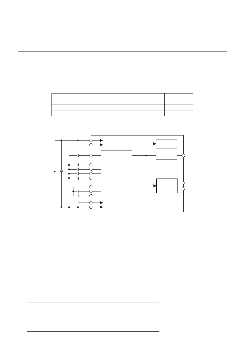
Table 2.1.1 Power supply circuits
Circuit
Oscillation and internal circuits
LCD driver
FSK demodulator
Power supply circuit
Oscillation system voltage regulator
LCD system voltage circuit
Analog system power supply
Output voltage
V
D1
V
C1
–V
C5
AV
DD
, AV
DD
Note: • Do not drive external loads with the output voltage from the internal power supply circuits.
• See Chapter 7, "Electrical Characteristics", for voltage values and drive capability.
External
power
supply
V
D1
OSC1~4
COM0~16
SEG0~39
V
C1
V
C23
V
C4
V
C5
CA
CB
CC
V
D1
V
DD
AV
DD
AV
SS
V
SS
V
C1
~ V
C5
+
-
Internal
circuits
Oscillation
circuit
LCD system
voltage circuit
Oscillation system
voltage regulator
LCD driver
Fig. 2.1.1 Configuration of power supply
2.1.1 Voltage
D1
> for oscillation circuit and internal circuits
V
D1
is a voltage for the oscillation circuit and the internal logic circuits, and is generated by the oscillation
system voltage regulator for stabilizing the oscillation. The V
D1
voltage is fixed at 2.1 V, so it is not
necessary to control by software.
2.1.2 Voltage
C1
–V
C5
> for LCD driving
V
C1
, V
C23
, V
C4
and V
C5
are the LCD (1/4 bias) drive voltages generated by the LCD system voltage
circuit. These four output voltages can only be supplied to the externally expanded LCD driver.
The LCD system voltage circuit generates V
C23
with the voltage regulator built-in, and generates three
other voltages by boosting or reducing the voltage of V
C23
. Table 2.1.2.1 shows the V
C1
, V
C23
, V
C4
and V
C5
voltage values and boost/reduce status.
Table 2.1.2.1 LCD drive voltage when generated internally
LCD drive voltage
V
C1
V
C23
V
C4
V
C5
Boost/reduce status
V
C2
×
0.5
V
C2
(standard)
V
C2
×
1.5
V
C2
×
2
Voltage value [V]
1.13
2.25
3.38
4.50
Note: The LCD drive voltage can
be adjusted by the software
(see Section 4.7.5). Values
in the above table are
typical values.
Refer to Section 4.7, "LCD Driver", for control of the LCD drive voltage.
