4 pin description – Epson S1C63558 User Manual
Page 14

4
EPSON
S1C63558 TECHNICAL MANUAL
CHAPTER 1: OUTLINE
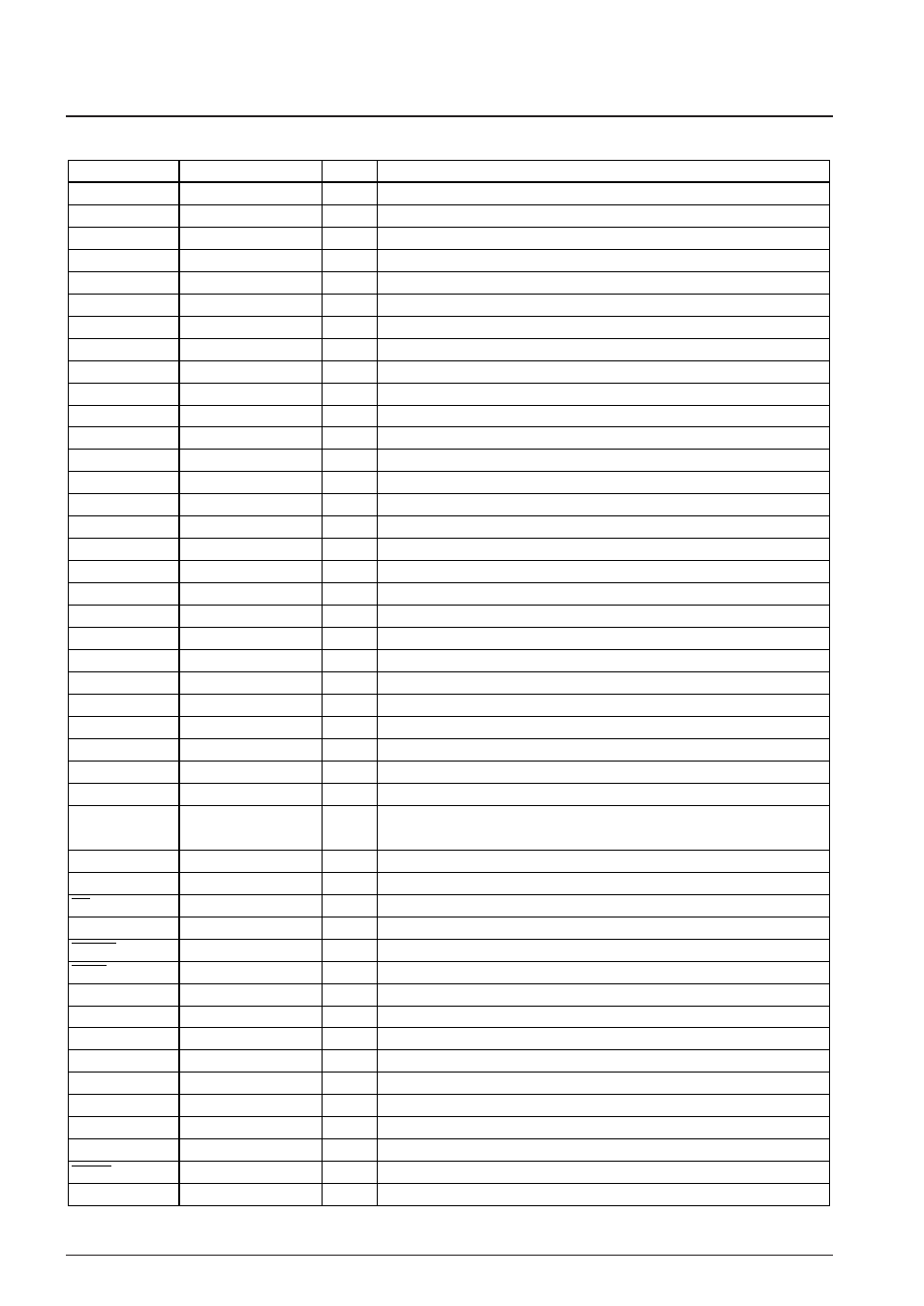
1.4 Pin Description
Table 1.4.1 Pin description
Pin name
V
DD
V
SS
V
D1
V
C1
–V
C5
CA–CC
OSC1
OSC2
OSC3
OSC4
K00–K03
K10–K13
P00–P03
P10–P13
P20
P21
P22
P23
P30–P33
R00
R01
R02
R03
R10
R11
R12
R13
R20–R23
COM0–COM7
COM8–COM16
(SEG47–SEG40)
SEG0–SEG39
SVD
DP
TONE
RESET
TEST
AV
DD
AV
SS
RDIN
TIP
RING
FB
BPOUT
CDIN
RDRC
V
REF
Pin No.
52
46
49
108–111
114–112
47
48
50
51
106–103
102–99
98, 95–93
92–89
88
87
86
85
84–81
70
69
68
67
66
63
62
61
60–57
45–38
115–123
37–33, 31–2, 128–124
107
56
55
53
54
80
76
74
79
78
77
72
71
73
75
Function
Power (+) supply pin
Power (–) supply pin
Oscillation system regulated voltage output pin
LCD system power supply pin (1/4 bias generated internally)
LCD system boosting/reducing capacitor connecting pin
Crystal oscillation input pin
Crystal oscillation output pin
Ceramic oscillation input pin
Ceramic oscillation output pin
Input port
Input port
I/O port
I/O port (switching to serial I/F (1) input/output is possible by software)
I/O port
I/O port
I/O port (switching to CL signal output is possible by software)
I/O port (switching to FR signal output is possible by software)
I/O port (switching to serial I/F (2) input/output is possible by software)
Output port (switching to XBZ signal output is possible by software)
Output port (switching to BZ signal output is possible by software)
Output port (switching to TOUT signal output is possible by software)
Output port (switching to FOUT signal output is possible by software)
Output port (switching to XTMUTE signal output is possible by software)
Output port (switching to XRMUTE signal output is possible by software)
Output port (switching to HDO signal output is possible by software)
Output port (switching to HFO signal output is possible by software)
Output port
LCD common output pin (1/8, 1/16, 1/17 duty can be selected by software)
LCD common output pin
or LCD segment output pin (mask option)
LCD segment output pin
SVD external voltage input pin
Dial pulse output pin
DTMF output pin
Initial reset input pin
Testing input pin
Power (+) supply pin for FSK demodulator
Power (-) supply pin for FSK demodulator
Ring detection input pin
TIP input pin
RING input pin
Input amplifier output pin
Band-pass filter output pin
Carrier detection input pin
I/O pin for connecting RC network
Reference voltage output pin (1/2 V
DD
)
I/O
–
–
–
–
–
I
O
I
O
I
I
I/O
I/O
I/O
I/O
I/O
I/O
I/O
O
O
O
O
O
O
O
O
O
O
O
O
I
O
O
I
I
–
–
I
I
I
O
O
I
I/O
O
